Materials for Printed/Flexible Electronics 2021-2031: Technologies, Applications, Market Forecastsプリンテッド/フレキシブルエレクトロニクスの素材 2021-2031年:技術、用途、市場予測 This IDTechEx Research report provides an extensive overview of the printed electronic materials market, covering materials for both existing and emerging flexible electronics applications. Inno... もっと見る
出版社
IDTechEx
アイディーテックエックス 出版年月
2021年4月19日
価格
お問い合わせください
ライセンス・価格情報/注文方法はこちら 納期
お問合わせください
ページ数
470
言語
英語
※価格はデータリソースまでお問い合わせください。
Summary
This IDTechEx Research report provides an extensive overview of the printed electronic materials market, covering materials for both existing and emerging flexible electronics applications. Innovative materials are a key enabling component of many printed/flexible electronics devices and range from organic semiconductors to quantum dots and from carbon nanotubes to conductive adhesives. By profiling multiple companies, we map the commercial adoption prospects and challenges for each material class and develop granular 10-year market forecasts across the entire printed electronic materials market.
IDTechEx has been researching the emerging printed electronics market since 2002. We have an unparalleled network of contacts throughout the printed/flexible electronics industry, enabling us to stay up-to-date with the technical and market developments. Many of these contacts in the materials space have been interviewed for this report, which builds on our masterclasses and workshops on 'printed electronic materials'.
Functional materials are obviously a fundamental part of the value chain for any emerging technology, but this is especially true of printed/flexible electronics since the materials need to combine electronic/semiconducting functionality with being flexible and/or solution processable as well as being stable and straight-forward to manufacture. This can be a significant technical challenge, leading to widespread innovation in materials development across both established and early stage companies.
This report covers many printed electronics materials, thus spanning multiple applications. More specifically, it covers:
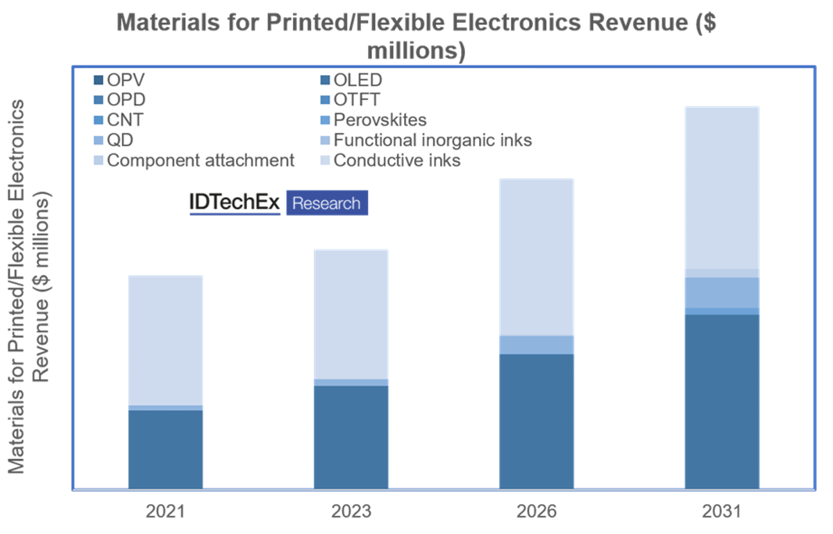
In total, IDTechEx Research finds that the printed electronics materials market will reach $6.9Bn in 2031.
This report provides a comprehensive overview of all solution processable materials that are compatible with printed/flexible electronics, with an emphasis on the most interesting emerging technologies. We identify the dominant technical and market narratives across printed electronic materials market. SWOT analysis is provided for each material category and for each profiled company, along with assessments of technological and commercial readiness.
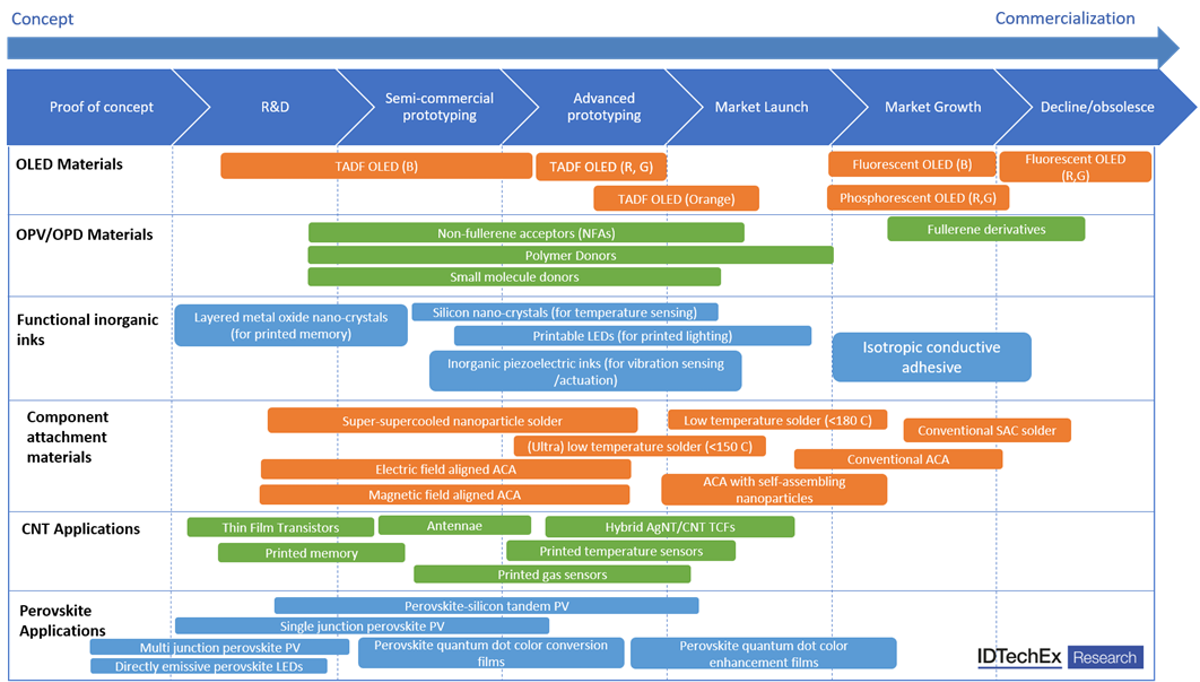
Organic light emitting diode materials (OLED materials)
OLEDs are the big commercial success story of printed/flexible electronics and indeed organic semiconductors; OLED displays are now a $30 bn market. However, technology never stands still and there is consistently innovation in both the emissive and host materials. Notable trends are the transition to Thermally Activated Delayed Fluorescence (TADF) materials and especially TADF molecules paired with fluorescent emitters and the continual quest for greater color purity. As the emissive layers and molecular architectures become more complex, we also see increasing adoption of material informatics to accompany experimental research in the development cycle.
Organic photovoltaic materials (OPV materials)
One of the original target applications for organic semiconductors, organic photovoltaics (OPV) has struggled to compete with the falling prices of silicon solar panels and more recently research efforts have largely shifted to thin film perovskite PV. However, the recent transition from fullerene derivatives to non-fullerene acceptors have led to increased efficiency and stability for OPVs. Combined with their well-known attributes of a tunable absorption spectrum, light weight and compatibility with roll-to-roll manufacturing, this has led to a partial renaissance with accelerating adoption for niche applications such as semi-transparent, indoor and building-integrated photovoltaics.
Organic photodetector materials (OPD materials)
Organic photodetectors are an emerging promising technology, since they enable both large area detectors and light detection at wavelengths greater than silicon. In terms of structure, OPDs are very similar to OPV devices, but optimized for spectral range and detectivity rather than power conversion efficiency. An especially promising approach is hybrid OPD-on-CMOS detectors, in which an OPD layer is used on a silicon readout circuit to extend the spectral sensitivity into the short-wave infra-red (SWIR) region. Such capabilities are very promising for machine vision in driver assistance/autonomous vehicles since long wavelength light is scattered less by dust and fog.
Organic thin film transistor materials (OTFT materials)
The prospect of printing integrated circuits using organic semiconductors has long been cited as the motivation for extensive research into these materials. However, despite multiple attempts to commercialize this technology it has proved very difficult to compete with silicon, ultimately leading to using silicon ICs with flexible/printed electronics - known as Flexible Hybrid Electronics. However, OTFTs are still viable as transistor backplanes for active matrix curved/flexible/foldable displays due to their more straightforward manufacturing. Indeed, we believe that OTFT backplanes can be deployed, albeit in a very limited capacity, in flexible electrophoretic e-readers.
Quantum dots
An alternative and fast-growing category of solution processable semiconductors is quantum dots (QDs). Regarding printable applications, quantum dots are currently used in color conversion/enhancement films to widen the color gamut of LCD displays, in the case of color conversion improve efficiency since light is re-emitted. This is commercially advantageous since LCD manufacturers are keen to differentiate what is now a largely commoditized product. Furthermore, quantum dots can also be used to sense photons in the short-wave infra-red spectral range, with hybrid QD-on-CMOS cameras now commercially available.
Photovoltaic perovskites
Arguably one of the most significant materials science discoveries of the last decade, organic/inorganic perovskites have demonstrated rapidly increasing photovoltaic (PV) efficiencies and are on the verge of commercialization with Oxford PV developing a multijunction silicon/perovskite tandem cell. While the perovskite active layer is generally synthesized in-situ, this requires very high-purity precursors, while devise require multiple specialized materials for charge transport layers. Although long term stability remains in question, perovskites could soon be used in LEDs and image sensors as well as photovoltaic, making this a technology to watch closely.
Carbon nanotubes (CNTs)
Carbon nanotubes (CNTs) have been known for many decades, but the moment of significant commercial growth is just approaching. Carbon nanotubes are very versatile, since they can be synthesized to be insulating, semiconducting or conducting, and produced in large quantities for bulk applications that to take advantage of their strength and thermal conductivity. Regarding the printable applications, transparent conductive films are a promising application. This involves combining CNTs with silver nanowires, which amongst other advantages improves conductivity for the same transparency as fewer silver nanowires are needed. Carbon nanotubes are also increasingly being deployed in printed sensors for parameters such as temperature, humidity, and even gases.
Component attachment materials
Alternatives to conventional SAC solder for component attachment are developing rapidly, with driving forces primarily a being a desire for lower processing temperatures to suit thermally fragile substrates such as PET, along with a need for more rapid processing and compatibility with fine I/O pitches. Material innovations include ultra-low temperature solder and field-aligned anisotropic conductive adhesives (ACA). Low temperature component attachment materials are especially important for the emerging manufacturing approach of flexible hybrid electronics (FHE) that aims to combine the desirable attributes of printed electronics with the capabilities of placed components.
Conductive inks
Conductive inks are one of the most developed markets in printed electronics, with screen-printed silver paste used to make conductive fingers on solar panels. However, there is still plenty of innovation in the sector, with the advent of particle-free, stretchable, and copper inks for applications as diverse as e-textiles and in-mold electronics (IME). We believe that IME offers scope for substantial growth, along with the emerging manufacturing approach of flexible hybrid electronics.
Functional inks
An emerging class of printable materials for electronic applications includes suspensions of inorganic materials. Inorganic nanocrystals, structured metal oxides and even functional LEDs can all be deposited from solution, enabling printing to be used as a manufacturing method for applications as diverse as lighting, temperature sensors and even memory. As materials develop additive manufacturing methods such as printing are likely to be increasing adopted across many applications, particularly where high-mix low-volume production is required.
Ten Year Market forecasts 2021-2031
Our detailed market forecasts cover each of the material categories outlined above, with breakdowns into further subcategories where relevant. Forecasts are provided in terms of both revenue and volume (in kg).
Materials for Printed/Flexible Electronics 2021-2031 provides a definitive assessment of this diverse and growing market. The market is enabled by specialized, functional materials and this report focuses on the material requirements, progress and opportunities. The technical analysis and interview-led approach brings the reader unbiased outlooks, benchmarking studies and player assessments across this diverse and expanding industry.
Table of Contents
株式会社 データリソース Data Resource, Inc.
電話:03-3582-2531
COPYRIGHT(C) 2011-2025 DATA RESOURCE, Inc. ALL RIGHTS RESERVED. |