世界各国のリアルタイムなデータ・インテリジェンスで皆様をお手伝い

フレキシブル&プリンテッドエレクトロニクス2023-2033年:予測、技術、市場


Flexible & Printed Electronics 2023-2033: Forecasts, Technologies, Markets

「フレキシブル&プリンテッドエレクトロニクス 2023-2033年: 予測、技術、市場」は、エレクトロニクスへの新たなアプローチにおけるトレンドとイノベーションを調査・評価したものです。IDTechExの広範なプ... もっと見る


出版社 出版年月 電子版価格 ページ数 言語
IDTechEx
アイディーテックエックス
2023年6月5日 US$7,000
電子ファイル(1-5ユーザライセンス)
ライセンス・価格情報・注文方法はこちら
314 英語

日本語のページは自動翻訳を利用し作成しています。


サマリー

「フレキシブル&プリンテッドエレクトロニクス 2023-2033年: 予測、技術、市場」は、エレクトロニクスへの新たなアプローチにおけるトレンドとイノベーションを調査・評価したものです。IDTechExの広範なプリント/フレキシブルエレクトロニクスに関するレポートポートフォリオを要約し、この発展途上の業界を長年にわたって追跡調査した結果をもとに、プリント/フレキシブルエレクトロニクス市場の5分野(自動車、消費財、エネルギー、ヘルスケア/ウェルネス、インフラ/ビルディング/産業)におけるイノベーション、機会、トレンドについて概説しています。この分析には、50の異なるアプリケーションの詳細な予測も含まれています。
 
さらに、プリンテッドフレキシブルエレクトロニクス市場の様々な側面における開発についても概説しています: 6種類の製造方法(インモールドエレクトロニクスやフレキシブルハイブリッドエレクトロニクスを含む)、5種類の材料(導電性インクや部品取り付け材料を含む)、4種類の部品(フレキシブルICを含む)。技術開発の方向性と商業化の成功を示す複数の事例が、技術的および商業的な準備の評価とともに提供されています。また、製造方法と導電性インクに関する追加予測も行っています。
 
プリンテッド/フレキシブルエレクトロニクスの動機
従来のエレクトロニクス製造は、銅ラミネートを選択的にエッチングしてPCB(プリント回路基板)上に導電性トレースを残すもので、確立されたユビキタス技術である。では、なぜプリント/フレキシブルエレクトロニクスが必要なのでしょうか?
 
主な利点は、フレキシブル(伸縮可能)なフォームファクターと大面積の生産能力であると言えるでしょう。ポリイミド基板にエッチングされた銅ラミネートを使用したフレキシブルPCBは確立されたアプローチですが、コンポーネントはしばしば、標準的なシート・ツー・シート方式で「リジッドアイランド」にマウントされています。
 
アプリケーションの可能性
従来のPCBと同様に、プリンテッド&フレキシブルエレクトロニクスは、多くの市場垂直方向でアプリケーションを見つけることができます。本レポートでは、5つの垂直市場ごとに市場を予測し、特定のアプリケーションごとにさらに細分化しています。最も商業的に有望で革新的なアプリケーションを例示し、基礎となるアプリケーションの現状と見通しを図解しています。
 
プリント/フレキシブルエレクトロニクスの柔軟性と伸縮性により、この技術はウェアラブルアプリケーションに非常に適している。電極や接点に導電性インクを使用したエレクトロニクス皮膚パッチはすでに発売されており、歩行モニタリング用のプリント感圧インソールもあります。
 
また、差別化のチャンスとして注目されている自動車内装も、大きな注目を集めているアプリケーション分野です。プリンテッド/フレキシブルエレクトロニクスは、タッチセンサー、暖房、照明などを統合した大面積のコンフォーマル機能を実現するのに適している。
 
もちろん、持続可能性の向上は多くの新技術の原動力であり、プリンテッドエレクトロニクスもその例に漏れない。有機太陽電池は、数年前までは困難な状況にありましたが、現在ではルネッサンスを迎えています。
フレキシブル&プリンテッドエレクトロニクス 2023-2033」に含まれるトピックス: 予測、技術、市場」に掲載されています。出典 IDTechEx
 
製造方法
プリンテッド/フレキシブル・エレクトロニクスの利点は、新しいアプリケーションの実現にとどまりません。積層銅の減法的除去を導電性インクの加法的堆積に置き換えた、根本的に異なる製造方法です。これにより、廃棄物が削減され、デジタル製造が容易になり、ラピッドプロトタイピングや簡単なデザイン調整といった関連する利点が得られます。
 
本レポートでは、完全積層3Dエレクトロニクスからインモールドエレクトロニクス、新たなデジタル印刷法まで、さまざまな製造イノベーションとその展望を評価しています。注目すべき事例、利点と課題、および以下を含みます。
 
材料イノベーション
材料イノベーションは、多くの新興ハードウェア技術を支えており、プリンテッドエレクトロニクスも例外ではありません。導電性インクがこの技術を支えており、数十社がさまざまな組成と属性を持つインクを開発しています。スクリーン印刷用の銀フレークベースの粘性インクが主流ですが、EMIシールドのような特定の用途では、ナノ粒子や粒子を含まないインクなどの代替品が人気を博しています。特に注目すべきは銅インクの開発で、銀インクと比較して大幅なコストダウンが期待できます。これは長い間の願望でしたが、技術開発によって酸化の問題がほぼ解決され、銅インクは商業的に採用される寸前まで来ています。
 
その他の特殊材料も、プリンテッド/フレキシブル・エレクトロニクスを実現する上で重要な役割を担っています。たとえば、超低温はんだやフィールドアライメント型異方性導電接着剤などの新しい部品取り付け材料は、LED のような部品を、安価で熱に弱い基板にしっかりと取り付けることができるようにします。さらに、多くのセンサーは、振動検知用の印刷可能な圧電ポリマーやイオン検知用の機能化カーボンナノチューブなど、特殊な材料を必要とします。
 
フレキシブルな部品
プリンテッドエレクトロニクスとフレキシブルエレクトロニクスの当初の構想は、集積回路を含む回路のあらゆる側面を印刷することでしたが、これはフレキシブルハイブリッドエレクトロニクス(FHE)にほぼ取って代わられました。このアプローチでは、プリンテッドロジックがシリコンに対抗するのは難しいと考え、集積回路を搭載しながら導電性トレースやセンサーなどの部品を印刷することで、「両者の良いとこ取り」を目指します。
 
もちろん、リジッドコンポーネントを搭載すると、薄膜フレキシブルフォームファクターはある程度損なわれます。特に大型のコンポーネントの場合はそうです。そのため、フレキシブルIC、バッテリー、ディスプレイ、さらにはセンサーなどを単独で製造し、フレキシブル基板に実装する機会があります。
 
フレキシブルエレクトロニクスの機能の多くと同様に、一般に、従来の性能指標の最適化よりも、フレキシブルなフォームファクターの実現、コストの削減、持続可能性の向上が重視されています。例えば、フレキシブル金属酸化物ICは、RFIDタグのコスト削減に貢献し、将来的にはスマートパッケージングアプリケーション向けにさらなる機能を追加することができます。
 
専門知識の構築
IDTechExは、10年以上にわたってプリンテッドエレクトロニクスとフレキシブルエレクトロニクス市場の開発を調査してきました。それ以来、世界中の主要なプレーヤーにインタビューを行い、FLEXやLOPECなどの会議に毎年参加し、複数のコンサルティングプロジェクトを提供し、このテーマに関するクラスやワークショップを開催するなど、技術および商業の発展に密着してきました。'Flexible & Printed Electronics 2023-2033: 技術、市場、予測」は、この経験と専門知識を活用し、この分野全体にわたるIDTechExの知識と洞察力をまとめたものです。


ページTOPに戻る


目次

1. エグゼクティブサマリー
1.1. プリンテッド/フレキシブル・エレクトロニクス:アナリストの視点(I)
1.2. プリンテッド/フレキシブルエレクトロニクス:アナリストの視点(II)
1.3. プリンテッドエレクトロニクス/フレキシブルエレクトロニクスとは?
1.4. プリンテッド/フレキシブル・エレクトロニクスの動機付け
1.5. プリンテッド/フレキシブルエレクトロニクスとハイプカーブ:製品市場への適合に向けた進展
1.6. プリンテッド/フレキシブルエレクトロニクス産業の展望をセグメント化する
1.7. 車載用プリンテッドフレキシブルエレクトロニクス:概要
1.8. 概要消費財におけるプリンテッド/フレキシブル・エレクトロニクス
1.9. 概要エネルギー分野におけるプリンテッド/フレキシブルエレクトロニクス
1.10. 概要ヘルスケア/ウェルネスにおけるプリンテッド/フレキシブル・エレクトロニクス
1.11. 概要インフラ/ビル/産業におけるプリンテッド/フレキシブルエレクトロニクス
1.12. プリンテッド/フレキシブルエレクトロニクス分野アプリケーション分野別予測(2023年、2028年、2033年)
1.13. プリンテッド/フレキシブルエレクトロニクス分野のアプリケーション分野別予測:2021年~2033年
1.14. プリンテッド/フレキシブルエレクトロニクスのアプリケーション分野別収益予測(2023年、2028年、2033年)
1.15. プリンテッド/フレキシブルエレクトロニクスのアプリケーション分野別収益予測(2023年、2028年、2033年)
1.16. プリンテッド/フレキシブルエレクトロニクスの製造方法:概要
1.17. プリンテッドエレクトロニクスは加法性だが、アナログでもデジタルでも可
1.18. 印刷方式を比較する:解像度とスループットの比較
1.19. 全体予想です:アナログ印刷方式
1.20. 全体予想です:デジタル印刷方式
1.21. プリンテッド/フレキシブルエレクトロニクスの製造方法:主な結論
1.22. プリンテッド・フレキシブル・エレクトロニクス用材料:概要
1.23. 全体的な予測です:導電性インクの数量(インクタイプ別セグメント)
1.24. 全体的な予測です:導電性インクの売上高(インクタイプ別内訳)
1.25. プリンテッド/フレキシブルエレクトロニクス用材料:主な結論
1.26. プリンテッド・フレキシブル・エレクトロニクス用部品:概要
1.27. プリンテッド/フレキシブルエレクトロニクス用部品:主な結論
2. イントロダクション
2.1. プリンテッドエレクトロニクス/フレキシブルエレクトロニクスとは?
2.2. プリンテッド/フレキシブル・エレクトロニクスの動機付け(I)
2.3. プリンテッド/フレキシブルエレクトロニクスとハイプカーブ:製品市場への適合に向けた進展
2.4. エレクトロニクス業界におけるプリンテッド/フレキシブル・エレクトロニクスへの関わり方
2.5. プリンテッドエレクトロニクス/フレキシブルエレクトロニクスを牽引するマクロトレンド:AI/機械学習による連続モニタリングの増加
2.6. プリンテッド/フレキシブルエレクトロニクスを牽引するマクロトレンド:差別化・カスタマイズへの欲求
2.7. プリンテッド/フレキシブルエレクトロニクスを牽引するマクロトレンド:サステナビリティの重要性
2.8. プリンテッド/フレキシブル・エレクトロニクスを牽引するマクロトレンド:アンビエントコンピューティングへの移行
3. 市場予測
3.1. 概要
3.1.1. 市場予測方法:アプリケーション
3.1.2. 市場予測の方法論:素材・部品・製造方法
3.1.3. プリンテッド/フレキシブルエレクトロニクス分野アプリケーション分野別予測(2023年、2028年、2033年)
3.1.4. プリンテッド/フレキシブルエレクトロニクス分野のアプリケーション分野別予測:2021年~2033年
3.1.5. プリンテッド/フレキシブルエレクトロニクスのアプリケーション分野別収益予測(2023年、2028年、2033年)
3.1.6. プリンテッド/フレキシブルエレクトロニクスのアプリケーション分野別収益予測(2023年、2028年、2033年)
3.2. 市場予測アプリケーション分野
3.2.1. プリンテッド/フレキシブルエレクトロニクスの車載用途:面積別(千m2)
3.2.2. プリンテッド/フレキシブルエレクトロニクスの自動車用途:売上高(百万米ドル)
3.2.3. プリンテッド/フレキシブルエレクトロニクスの消費財用途(面積別)(千m2
3.2.4. プリンテッド/フレキシブルエレクトロニクスの消費財用途:売上高(百万米ドル)
3.2.5. プリンテッド/フレキシブルエレクトロニクスのエネルギー用途(面積別)(千m2
3.2.6. プリンテッド/フレキシブルエレクトロニクスのエネルギー用途:売上高(百万米ドル)
3.2.7. プリンテッド/フレキシブルエレクトロニクスのヘルスケア/ウェルネス/アパレル用途:面積別(千m2)
3.2.8. プリンテッド/フレキシブルエレクトロニクスのヘルスケア/ウェルネス用途:売上高(百万米ドル)
3.2.9. プリンテッド/フレキシブルエレクトロニクスのインフラ/建築/産業用途の面積別推移(千m2)
3.2.10. プリンテッド/フレキシブルエレクトロニクスのインフラ/建築/産業用途の売上高(百万米ドル)
3.3. 市場予測です:製造方法
3.3.1. 全体予想です:アナログ印刷方式
3.3.2. 全体予想です:アナログ印刷方式割合
3.3.3. 全体予想です:デジタル印刷方式
3.3.4. 全体予想です:デジタル印刷方式割合
3.4. 市場予測です:導電性インク
3.4.1. 全体的な予測です:導電性インクの数量(インクタイプ別セグメント)
3.4.2. 全体的な予測です:導電性インクの売上高(インクタイプ別内訳)
4. アプリケーション分野の概要
4.1. アプリケーション分野の紹介
4.1.1. プリンテッド/フレキシブルエレクトロニクスの応用分野
4.2. アプリケーション分野自動車
4.2.1. プリンテッド/フレキシブルエレクトロニクスの車載用途はじめに
4.2.2. 業界の変遷に伴い、新たな差別化要因が求められる
4.2.3. プリント/フレキシブルエレクトロニクスによるコスト差別化、コスト削減の実現
4.2.4. 車内インテリアのトレンドから生まれるプリンテッド/フレキシブルエレクトロニクスの可能性
4.2.5. HMI用プリンテッドエレクトロニクスの実用化が進む
4.2.6. 車載用面状発熱体としてプリントヒーターへの注目度が高まる
4.2.7. 車載用透明アンテナで窓の機能化を実現
4.2.8. 車載用プリンテッド/フレキシブルエレクトロニクス:SWOT分析
4.2.9. 自動車内装におけるプリンテッド/フレキシブル・エレクトロニクス:レディネス・レベル評価
4.2.10. 車両外装のプリンテッド/フレキシブル・エレクトロニクス:レディネス・レベル評価
4.2.11. プリンテッド/フレキシブルエレクトロニクスの自動車への応用:結論
4.3. アプリケーション分野消費財
4.3.1. プリンテッド/フレキシブルエレクトロニクスの消費財用途:はじめに
4.3.2. 天然素材にエレクトロニクスを埋め込む
4.3.3. 導電性ペーストの押し出しとインクジェット印刷による3次元表面へのエレクトロニクス化
4.3.4. アンテナ用導電性ペーストの押し出し成形
4.3.5. 印刷されたRFIDアンテナは、牽引力に苦戦:銅インクが解決策になるか?
4.3.6. フレキシブルハイブリッドエレクトロニクスを搭載したスマートパッケージング
4.3.7. スマートパッケージング用有機EL
4.3.8. 消費財向けプリンテッド/フレキシブルエレクトロニクス:SWOT分析
4.3.9. プリンテッド/フレキシブルエレクトロニクスの消費財への応用:結論
4.4. アプリケーション分野エネルギー
4.4.1. プリンテッド/フレキシブルエレクトロニクスのエネルギー応用:はじめに
4.4.2. 太陽光発電用導電性ペースト
4.4.3. フレーク状導電性インク、太陽電池の代替接続技術で逆風にさらされる
4.4.4. 有機薄膜太陽電池の普及が進む
4.4.5. 有機薄膜太陽電池(OPV)のルネサンスは続く
4.4.6. ペロブスカイト太陽電池、シリコンに匹敵する急速な効率向上を示す
4.4.7. 薄膜フレキシブルPVの実用化を目指す各社
4.4.8. 薄膜ペロブスカイト太陽電池のロードマップ
4.4.9. エネルギー用プリンテッド/フレキシブルエレクトロニクス:SWOT分析
4.4.10. エネルギー用プリンテッド/フレキシブル・エレクトロニクス:結論
4.5. アプリケーション分野ヘルスケア/ウェルネス
4.5.1. プリンテッド/フレキシブルエレクトロニクスのヘルスケア/ウェルネスへの応用:はじめに
4.5.2. 電気化学バイオセンサーは、プリンテッドエレクトロニクスを利用したシンプルなセンシングメカニズムです。
4.5.3. 生体情報を継続的にモニタリングする皮膚パッチへの関心が続いています。
4.5.4. 材料メーカーの協力により、ウェアラブル皮膚パッチの大規模な試験が可能になった
4.5.5. 病院内への応用は有望だが、困難が残る
4.5.6. 電子テキスタイルとウェアラブルセンシングは、洗濯性の問題を克服することを目指しています。
4.5.7. ウェアラブルエレクトロニクス用ストレッチャブルインクとしての液体金属合金の利用が進む
4.5.8. 生体液用印刷pHセンサー
4.5.9. ウェアラブル電極の主な要件
4.5.10. ウェアラブル/メディカル向け製造の需要増により、拡張計画が進む
4.5.11. 医薬品のコンプライアンスを向上させるスマートパッケージング
4.5.12. ヘルスケア/ウェルネスアプリケーション向けプリンテッド/フレキシブルエレクトロニクス:SWOT分析
4.5.13. ヘルスケア/ウェルネスアプリケーション向けプリンテッド/フレキシブルエレクトロニクス:SWOT分析(二)
4.5.14. ヘルスケア/ウェルネスアプリケーション向けプリンテッド/フレキシブルエレクトロニクス:準備レベル
4.5.15. ヘルスケア/ウェルネスアプリケーション向けのプリンテッド/フレキシブルエレクトロニクス:結論
4.6. アプリケーション分野インフラ/ビル/産業
4.6.1. プリンテッド/フレキシブルエレクトロニクスのインフラ/ビル/産業用アプリケーションはじめに
4.6.2. ハイブリッドエレクトロニクスによる産業用資産のトラッキング/モニタリング
4.6.3. 床や壁パネルに組み込まれた静電容量式センサー
4.6.4. プリンテッドエレクトロニクスが実現するコスト効率の高い建物・環境センシング
4.6.5. 集積化された透明アンテナや再構成可能なインテリジェントサーフェスの構築
4.6.6. パッシブRISのための素材選び
4.6.7. 統合エレクトロニクスが実現する産業用モニタリング
4.6.8. 統合されたエレクトロニクスが、カスタマイズ可能なインテリアを約束する
4.6.9. 建築/インフラ/産業用途のプリンテッド/フレキシブルエレクトロニクス:SWOT分析(I)
4.6.10. 建築/インフラ/産業用途のプリンテッド/フレキシブルエレクトロニクス:SWOT分析(二)
4.6.11. インフラ/ビル/産業用アプリケーションのためのプリンテッド/フレキシブルエレクトロニクス:結論
5. プリント/フレキシブル・エレクトロニクスの製造方法:概要
5.1. はじめに
5.1.1. プリンテッド/フレキシブルエレクトロニクスの製造方法:概要
5.1.2. プリンテッドエレクトロニクスは加法性だが、アナログでもデジタルでも可
5.1.3. 印刷方式を比較する:解像度とスループットの比較
5.1.4. プリンテッド/フレキシブルエレクトロニクスの信頼性確保は重要だ
5.1.5. 製造業のデジタル化により、プリンテッド・エレクトロニクス・アズ・ア・サービスが実現します;
5.2. 製造方法:3Dエレクトロニクス
5.2.1. 3Dエレクトロニクス:はじめに
5.2.2. アディティブエレクトロニクスと3次元への移行
5.2.3. 3D/アディティブエレクトロニクスは、複数の長さスケールにまたがっている。
5.2.4. 完全3Dプリンターによるエレクトロニクスのプロセスステップ
5.2.5. 新規参入企業により、完全添加型エレクトロニクスへの関心が高まる
5.2.6. 完全積層造形3Dエレクトロニクスの優位性
5.2.7. 3Dエレクトロニクス:SWOT分析
5.2.8. 積層造形技術のレディネス・レベル
5.2.9. 3Dエレクトロニクス:結論
5.3. 製造方法について:アナログ製造
5.3.1. アナログ印刷です:はじめに
5.3.2. 従来のスクリーン印刷会社がプリント/フレキシブルエレクトロニクスを採用し続ける
5.3.3. スクリーン印刷の解像度を向上させる
5.3.4. ラップアラウンド電極の高精細スクリーン印刷。
5.3.5. Clichéベースの印刷方式。
5.3.6. リバースオフセット印刷で実現する高解像度
5.3.7. アナログ印刷です:SWOT分析
5.3.8. アナログ印刷方式のベンチマーキング
5.3.9. アナログ印刷方式の技術的・商業的準備レベル
5.3.10. 概要:アナログの印刷方式
5.4. 製造方法:デジタル印刷
5.4.1. デジタル印刷です:はじめに
5.4.2. デジタル印刷は、複数の長さスケールをカバーする
5.4.3. デジタル印刷方式のベンチマーキング
5.4.4. 成膜方法の比較
5.4.5. レーザー誘起前方移動(LIFT)の動作メカニズム
5.4.6. デジタルマニュファクチャリングが引き続き注目されている
5.4.7. 高解像度印刷の革新的な技術
5.4.8. アディティブエレクトロニクスによるプロトタイピングの比重が高まる
5.4.9. デジタル印刷です:SWOT分析
5.4.10. デジタル印刷です:レディネス・レベル
5.4.11. デジタル印刷です:結論
5.5. 製造方法です:フレキシブルハイブリッドエレクトロニクス
5.5.1. フレキシブルハイブリッドエレクトロニクス:はじめに
5.5.2. FHEは、両方の良いところを取り入れたアプローチをしています。
5.5.3. フレキシブルハイブリッドエレクトロニクス(FHE)
5.5.4. 従来型とプリンテッド/フレキシブルエレクトロニクスのメリットを比較する
5.5.5. FHEのバリューチェーン:多くの素材と技術
5.5.6. 伸縮性インクのもう一つの応用例「ウェアラブルスキンパッチ
5.5.7. 従来の箱型からフレキシブルなハイブリッド・エレクトロニクスへの発展は困難である
5.5.8. コンディションモニタリング用マルチモーダルセンサアレイ
5.5.9. マルチセンサーによる無線資産追跡システムで、FHEの可能性を示す
5.5.10. フレキシブル・ハイブリッド・エレクトロニクス(FHE)の新たな受託メーカーが登場
5.5.11. フレキシブルハイブリッドエレクトロニクス(FHE):SWOT分析
5.5.12. フレキシブルハイブリッドエレクトロニクス(FHE):結論
5.6. Manufacturing methods:インモールドエレクトロニクス
5.6.1. インモールドエレクトロニクス(IME):はじめに
5.6.2. IME製造工程フロー
5.6.3. スマートサーフェス製造方法の比較
5.6.4. IME製造技術の細分化
5.6.5. IMEの商業的メリット
5.6.6. IMEバリューチェーン-インモールドデコレーション(IMD)の発展形として
5.6.7. IMEバリューチェーンの概要
5.6.8. SMD部品を内蔵しないインモールドエレクトロニクスが急速に普及しています。
5.6.9. 概要IMEのための専門的な資料の
5.6.10. Materials for IME: A portfolio approach
5.6.11. 銀フレークベースのインクがIMEを席巻
5.6.12. 概要IMEとサステナビリティの
5.6.13. インモールドエレクトロニクス:SWOT分析:
5.6.14. 結論IME業界向け(I)
5.7. Manufacturing methods:R2R製造
5.7.1. R2R製造:はじめに
5.7.2. CanR2R製造 be used for high mix low volume (HMLV)?
5.7.3. ロールツーロール製造の主な商業的課題は何でしょうか?
5.7.4. エレクトロニクスのR2Rパイロット/プロダクションラインの例
5.7.5. R2Rエレクトロニクスによる商業印刷圧力センサーの製作
5.7.6. フレキシブル・ハイブリッド・エレクトロニクス(FHE)の受託製造会社の出現
5.7.7. Applying 'Industry 4.0' to printed electronics with in-line monitoring
5.7.8. R2Rエレクトロニクス製造の応用例
5.7.9. R2R製造:SWOT分析
5.7.10. R2R製造:レディネス・レベル
5.7.11. R2R製造:結論
6. MATERIALS FOR PRINTED/FLEXIBLE ELECTRONICS: OVERVIEW
6.1. はじめに
6.1.1. プリンテッド・フレキシブル・エレクトロニクス用材料:概要
6.1.2. 材料サプライヤーの商品化戦略(I)
6.1.3. 材料サプライヤーの商品化戦略(二)
6.2. Materials:部品取り付け部材s
6.2.1. 部品取り付け部材:はじめに
6.2.2. アタッチメント素材による差別化要因
6.2.3. 低温はんだで熱に弱い基板を実現。
6.2.4. 電気部品取り付け材料の比較
6.2.5. FHE回路開発には、耐久性と効率的な部品取り付けが重要である
6.2.6. フィールドアライメント型異方性導電接着剤が製品化へ
6.2.7. フォトニックソルダリングの普及が進む
6.2.8. 部品取り付け部材s (プリント/フレキシブルエレクトロニクス用):SWOT分析
6.2.9. 部品取り付け部材s:レディネス・レベル
6.2.10. 部品取り付け部材sプリント/フレキシブルエレクトロニクス用s:結論
6.3. Materials:導電性インクs
6.3.1. 導電性インクs:はじめに
6.3.2. Conductivity requirements by application
6.3.3. Challenges of comparing conductive inks
6.3.4. 導電性インクの技術区分s
6.3.5. 導電性インク companies segmented by conductive material
6.3.6. 市場の進化と新たな可能性s
6.3.7. What are the key growth markets for conductive inks?
6.3.8. Balancing differentiation and ease of adoption
6.3.9. Interest in novel conductive inks continues
6.3.10. Copper inks gaining traction but not yet widely deployed
6.3.11. Companies continue to develop and market stretchable/thermoformable materials
6.3.12. 導電性インクs:SWOT分析
6.3.13. 導電性インクs:レディネス・レベル assessment
6.3.14. 導電性インクs:結論
6.4. Materials: Printable semiconductors
6.4.1. Printable semiconducting materials:はじめに
6.4.2. Organic semiconductors: Advantages and disadvantages
6.4.3. Non-fullerene acceptors support OPV renaissance for non-standard applications
6.4.4. Substantial opportunities for OPD and QD materials in hybrid image sensing
6.4.5. Interest in OTFTs continues despite struggles
6.4.6. Printable semiconductors:SWOT分析
6.4.7. レディネス・レベル of printed semiconductors (organic and perovskite applications)
6.4.8. Printable semiconductors:結論
6.5. Materials: Printable sensing materials
6.5.1. Printable sensing materials:はじめに
6.5.2. Drivers for printed/flexible sensors
6.5.3. 概要 of specific printed/flexible sensor types
6.5.4. Polymeric piezoelectric materials receive increasing interest
6.5.5. Sensing for industrial IoT
6.5.6. Sensing for wearables/AR
6.5.7. Companies looking to incorporate printed/ flexible sensors often require a complete solution
6.5.8. Printable sensor materials:SWOT分析
6.5.9. Printed sensor materials:レディネス・レベル assessment
6.5.10. Printed sensor materials:結論
6.6. Materials and components: Substrates
6.6.1. Substratesプリント/フレキシブルエレクトロニクス用s:はじめに
6.6.2. Cost and maximum temperature are correlated
6.6.3. Properties of typical flexible substrates
6.6.4. Comparing stretchable substrates
6.6.5. Thermoset stretchable substrate used in multiple development projects
6.6.6. Paper substrates: Advantages and disadvantages
6.6.7. Substrates:結論
7. プリンテッド/フレキシブルエレクトロニクス用コンポーネントの概要
7.1. はじめに
7.1.1. プリンテッド・フレキシブル・エレクトロニクス用部品:概要
7.1.2. Component suppliers collaborate on smart packaging and shelf level marketing
7.1.3. Using a thin film component as a substrate: A cost-reduction strategy
7.2. Components: Electrophoretic / electrochromic displays
7.2.1. Electrophoretic / electrochromic displays:はじめに
7.2.2. 車体外装用カラーE-inks
7.2.3. Electrochromic display architecture
7.2.4. Electrochromic display in packaging
7.2.5. Electrophoretic / electrochromic displays:SWOT分析
7.2.6. Electrophoretic / electrochromic displays:レディネス・レベル assessment
7.2.7. Electrophoretic / electrochromic displays:結論
7.3. Components:フレキシブルバッテリーs
7.3.1. フレキシブルバッテリーs:はじめに
7.3.2. 'Thin', 'flexible' and 'printed' are separate properties
7.3.3. Major battery company targets printed/flexible batteries for smart packaging
7.3.4. Printed flexible batteries in development for smart packaging
7.3.5. プリンテッド・フレキシブルバッテリーの技術ベンチマーキングs
7.3.6. フレキシブルバッテリーs:SWOT分析
7.3.7. プリンテッド・フレキシブルバッテリーのアプリケーションロードマップs
7.3.8. フレキシブルバッテリーs:結論
7.4. Components:フレキシブルICs
7.4.1. フレキシブルICs:はじめに
7.4.2. Fully printed ICs have struggled to compete with silicon
7.4.3. Current approaches to printed logic
7.4.4. Embedding thinned silicon ICs in polymer
7.4.5. Embedding both thinned ICs and redistribution layer in flexible substrate
7.4.6. Investment into metal oxide ICs continues
7.4.7. フレキシブルICs:SWOT分析
7.4.8. フレキシブルICのロードマップs
7.4.9. フレキシブルICs:結論
7.5. Components: Flexible PV for energy harvesting
7.5.1. Flexible PV for energy harvesting:はじめに
7.5.2. Epishine is leading the way in solar powered IoT
7.5.3. Exeger's partnerships show promising future of DSSCs
7.5.4. Perovskite PV could be cost-effective alternative for wireless energy harvesting
7.5.5. Saule Technologies: Perovskite PV developer for indoor electronics
7.5.6. Flexible PV for energy harvesting:レディネス・レベル assessment
7.5.7. Flexible PV for energy harvesting:SWOT分析
7.5.8. Flexible PV for energy harvesting:
8. 会社概要
8.1. ACI素材s
8.2. アグファ
8.3. ビーエフシー
8.4. C3 Nano
8.5. Chasm
8.6. ケムキューブド
8.7. コアテマ
8.8. コッププリント
8.9. 消費者物価指数
8.10. ドゥマイクロ
8.11. デュポン
8.12. エランタs
8.13. エレクトロリンクs
8.14. GEヘルスケア
8.15. ヘンケル
8.16. ヘレウs
8.17. インクロン
8.18. イノベーションラボ
8.19. イヌル
8.20. アイオーテック
8.21. アイソルグ
8.22. ライアー
8.23. リキッドワイヤー
8.24. Nano Dimension
8.25. オプトメック
8.26. ポリイック
8.27. プラグマティック
8.28. プリントシービー
8.29. PVNanoCell
8.30. サラロン
8.31. スクリーンテック
8.32. サンケミカル
8.33. スニュー
8.34. Symbiose
8.35. タクトテック
8.36. トラキック
8.37. 通信事業者
8.38. ウィリオット
8.39. Ynvisible
8.40. Ynvisible/Evonik/EpishineContact IDTechEx

1


ページTOPに戻る


Summary

この調査レポートでは、2023-2033年の完全積層3Dエレクトロニクスからインモールドエレクトロニクス、新たなデジタル印刷法まで、さまざまな製造イノベーションとその展望について詳細に調査・分析しています。
 
主な掲載内容(目次より抜粋)
  • 市場予測
  • アプリケーション分野の概要
  • プリンテッド/フレキシブルエレクトロニクスの製造方法: 概要
  • プリンテッド/フレキシブルエレクトロニクス用材料 概要
  • プリンテッド/フレキシブルエレクトロニクス用コンポーネントの概要
  • 会社概要
 
Report Summary
'Flexible & Printed Electronics 2023-2033: Forecasts, Technologies, Markets' explores and evaluates the trends and innovations across this emerging approach to electronics. By summarizing IDTechEx's extensive printed/flexible electronics report portfolio, and drawing on years of following this developing industry, the report outlines innovations, opportunities, and trends across 5 sectors of the printed and flexible electronics market: automotive, consumer goods, energy, healthcare/wellness, and infrastructure/buildings/industrial. This analysis includes granular forecasts of 50 distinct applications.
 
Additionally, the report outlines developments across multiple aspects of the printed and flexible electronics market: 6 distinct manufacturing modalities (including in-mold electronics and flexible hybrid electronics), 5 material types (including conductive inks and component attachment materials) and 4 component types (including flexible ICs). Multiple examples showing technology development directions and successful commercialization are provided, along with assessments of technological and commercial readiness. Additional forecasts for manufacturing methods and conductive inks are also provided.
 
Motivation for printed/flexible electronics
Conventional electronics manufacturing, in which copper laminate is selectively etched to leave conductive traces on a PCB (printed circuit board), is a well-established and ubiquitous technology. So why is printed/flexible electronics needed?
 
Arguably the main benefits are the flexible (and potentially stretchable) form factor combined with the ability to produce large areas. While flexible PCBs using etched copper laminate on a polyimide substrate are an established approach, components are often mounted on 'rigid islands' using standard sheet-to-sheet methods.
 
Application opportunities
As with conventional PCBs, printed and flexible electronics finds applications in many market verticals. The report forecasts the market for each of 5 verticals, with further segmentation by specific application. Illustrative examples showcase the most commercially promising and innovative applications, while the status and prospects of the underlying applications are illustrated.
 
The flexibility and stretchability of printed/flexible electronics makes the technology extremely well suited to wearable applications. Electronics skin patches utilizing conductive inks for electrodes and contacts are already available, as are printed pressure sensitive insoles for gait monitoring.
 
Another application sector seeing extensive traction is automotive interiors, which is increasingly regarded as an opportunity for differentiation. Printed/flexible electronics is well suited to producing large area, conformal functionality to enable integrated touch sensing, heating, and lighting.
 
Improving sustainability is of course a driver for many emerging technologies, and printed electronics is not different. After some challenging years organic photovoltaics is seeing a renaissance, with
 
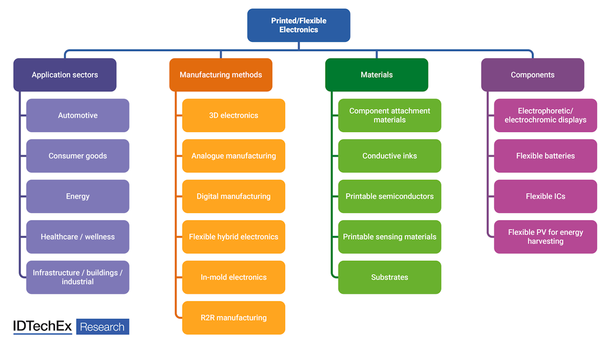
Topics included within the 'Flexible & Printed Electronics 2023-2033: Forecasts, Technologies, Markets'. Source IDTechEx
 
Manufacturing methods
The benefits of printed/flexible electronics go beyond enabling new applications. It is a fundamentally different approach to manufacturing, replacing subtractive removal of laminated copper with additive deposition of conductive ink. This reduces waste and facilitates digital manufacturing with the associated benefits of rapid prototyping and straightforward design adjustments.
 
The report evaluates a range of manufacturing innovations and their prospects, ranging from fully additive 3D electronics to in-mold electronics and emerging digital printing methods. This includes notable examples, benefits and challenges, and
 
Material innovations
Material innovations underpin many emerging hardware technologies, and printed electronics is no exception. Conductive inks underpin the technology, with dozens of companies developing inks with a range of compositions and attributes. Viscous silver-flake based ink for screen printing dominates, but alternatives such as nano-particle and particle-free inks are gaining traction for specific applications such as EMI shielding. An especially notable trend is the development of copper ink, which promises a substantial cost reduction over its silver counterparts. This has long been an aspiration, but technical developments have largely resolved difficulties with oxidation leaving copper inks on the verge of commercial adoption.
 
Other specialty materials also play an important role in enabling printed/flexible electronics. For example, emerging component attachment materials such as ultra-low temperature solder and field-aligned anisotropic conductive adhesives enable components such as LEDs to be securely attached to cheaper, thermally fragile substrates. Furthermore, many sensors require specialist materials, such as printable piezoelectric polymers for vibration sensing and functionalized carbon nanotubes for ion detection.
 
Flexible components
While the original vision for printed and flexible electronics was to print every aspect of the circuit, including the integrated circuit, this has largely been supplanted by flexible hybrid electronics (FHE). This approach accepts that printed logic will struggle to compete with silicon, instead aiming for the 'best of both worlds' by printing conductive traces and potentially components such as sensors while mounting integrated circuits.
 
Of course, mounting rigid components compromises the thin-film flexible form factor to some extent, especially for larger components. As such, there is an opportunity for flexible ICs, batteries, displays and even some sensors that are manufactured independently and then mounted onto flexible substrates.
 
As with much of the functionality within flexible electronics, the emphasis is generally on achieving a flexible form factor, reducing costs, and improving sustainability rather than optimizing conventional performance metrics. For example, flexible metal oxide ICs can help reduce the costs of RFID tags, and in the future add more functionality for smart packaging applications.
 
Building on expertise
IDTechEx has been researching developments in the printed and flexible electronics market for well over a decade. Since then, we have stayed close to technical and commercial developments, interviewing key players worldwide, annually attending conferences such as FLEX and LOPEC, delivering multiple consulting projects, and running classes/ workshops on the topic. 'Flexible & Printed Electronics 2023-2033: Technologies, Markets, Forecasts' utilizes this experience and expertise to summarize IDTechEx's knowledge and insight across the entire field.


ページTOPに戻る


Table of Contents

1. EXECUTIVE SUMMARY
1.1. Printed/flexible electronics: Analyst viewpoint (I)
1.2. Printed/flexible electronics: Analyst viewpoint (II)
1.3. What is printed/flexible electronics?
1.4. Motivation for printed/flexible electronics
1.5. Printed/flexible electronics and the hype curve: progressing towards product market fit
1.6. Segmenting the printed/flexible electronics industry landscape
1.7. Printed/flexible electronics in automotive applications: Overview
1.8. Overview: Printed/flexible electronics in consumer goods
1.9. Overview: Printed/flexible electronics in the energy sector
1.10. Overview: Printed/flexible electronics in healthcare / wellness
1.11. Overview: Printed/flexible electronics in infrastructure / buildings / industrial
1.12. Printed/flexible electronics area forecast by application sector (2023, 2028, 2033)
1.13. Printed/flexible electronics area forecast by application sector: 2021 - 2033
1.14. Printed/flexible electronics revenue forecast by application sector (2023, 2028, 2033)
1.15. Printed/flexible electronics revenue forecast by application sector (2023, 2028, 2033)
1.16. Manufacturing methods for printed/flexible electronics: Overview
1.17. Printed electronics is additive, but can be analogue or digital
1.18. Comparison of printing methods: Resolution vs throughput
1.19. Overall forecast: Analogue printing methods
1.20. Overall forecast: Digital printing methods
1.21. Manufacturing methods for printed/flexible electronics: Key conclusions
1.22. Materials for printed/flexible electronics: Overview
1.23. Overall forecast: Conductive ink volume (segmented by ink type)
1.24. Overall forecast: Conductive ink revenue (segmented by ink type)
1.25. Materials for printed/flexible electronics: Key conclusions
1.26. Components for printed/flexible electronics: Overview
1.27. Components for printed/flexible electronics: Key conclusions
2. INTRODUCTION
2.1. What is printed/flexible electronics?
2.2. Motivation for printed/flexible electronics (I)
2.3. Printed/flexible electronics and the hype curve: progressing towards product market fit
2.4. Engagement with printed/flexible electronics from the wider electronics industry
2.5. Macro-trends driving printed/flexible electronics: Increased use of AI / machine learning for continuous monitoring
2.6. Macro-trends driving printed/flexible electronics: Desire for differentiation and customization
2.7. Macro-trends driving printed/flexible electronics: Importance of sustainability
2.8. Macro-trends driving printed/flexible electronics: Transition towards ambient computing
3. MARKET FORECASTS
3.1. Overview
3.1.1. Market forecasting methodology: Applications
3.1.2. Market forecasting methodology: Materials, components and manufacturing methods
3.1.3. Printed/flexible electronics area forecast by application sector (2023, 2028, 2033)
3.1.4. Printed/flexible electronics area forecast by application sector: 2021 - 2033
3.1.5. Printed/flexible electronics revenue forecast by application sector (2023, 2028, 2033)
3.1.6. Printed/flexible electronics revenue forecast by application sector (2023, 2028, 2033)
3.2. Market forecasts: Application sectors
3.2.1. Automotive applications of printed/flexible electronics by area (thousand m2)
3.2.2. Automotive applications of printed/flexible electronics by revenue (USD millions)
3.2.3. Consumer goods applications of printed/flexible electronics by area (thousand m2)
3.2.4. Consumer goods applications of printed/flexible electronics by revenue (USD millions)
3.2.5. Energy applications of printed/flexible electronics by area (thousand m2)
3.2.6. Energy applications of printed/flexible electronics by revenue (USD millions)
3.2.7. Healthcare/wellness/apparel applications of printed/flexible electronics by area (thousand m2)
3.2.8. Healthcare/wellness applications of printed/flexible electronics by revenue (USD millions)
3.2.9. Infrastructure/buildings/industrial applications of printed/flexible electronics by area (thousand m2)
3.2.10. Infrastructure/buildings/industrial applications of printed/flexible electronics by revenue (USD millions)
3.3. Market forecasts: Manufacturing methods
3.3.1. Overall forecast: Analogue printing methods
3.3.2. Overall forecast: Analogue printing methods (proportion)
3.3.3. Overall forecast: Digital printing methods
3.3.4. Overall forecast: Digital printing methods (proportion)
3.4. Market forecasts: Conductive inks
3.4.1. Overall forecast: Conductive ink volume (segmented by ink type)
3.4.2. Overall forecast: Conductive ink revenue (segmented by ink type)
4. OVERVIEW OF APPLICATION SECTORS
4.1. Introduction to application sectors
4.1.1. Application sectors for printed/flexible electronics
4.2. Application sectors: Automotive
4.2.1. Automotive applications for printed/flexible electronics: Introduction
4.2.2. Industry transitions require new differentiators
4.2.3. Printed/flexible electronics enables cost differentiation and/or cost reduction
4.2.4. Printed/flexible electronics opportunities from car interior trends
4.2.5. Printed electronics for HMI gains commercial traction
4.2.6. Increasing interest in printed heaters for surface heating in vehicles
4.2.7. Automotive transparent antennas enable windows to be functionalized
4.2.8. Printed/flexible electronics for automotive applications: SWOT analysis
4.2.9. Printed/flexible electronics in vehicle interiors: Readiness level assessment
4.2.10. Printed/flexible electronics in vehicle exteriors: Readiness level assessment
4.2.11. Automotive applications for printed/flexible electronics: Conclusions
4.3. Application sectors: Consumer goods
4.3.1. Consumer goods applications for printed/flexible electronics: Introduction
4.3.2. Embedding electronics in natural materials
4.3.3. Electronics on 3D surfaces with extruded conductive paste and inkjet printing
4.3.4. Extruded conductive paste for antennas
4.3.5. Printed RFID antennas struggle for traction: Is copper ink a solution?
4.3.6. Smart packaging with flexible hybrid electronics
4.3.7. OLEDs for smart packaging
4.3.8. Printed/flexible electronics for consumer goods: SWOT analysis
4.3.9. Consumer goods applications for printed/flexible electronics: Conclusions
4.4. Application sectors: Energy
4.4.1. Energy applications for printed/flexible electronics: Introduction
4.4.2. Conductive pastes for photovoltaics
4.4.3. Flake-based conductive inks face headwind from alternative solar cell connection technology
4.4.4. Organic photovoltaics gains traction
4.4.5. Renaissance of organic photovoltaics (OPV) continues
4.4.6. Perovskite PV shows rapid efficiency gains to be comparable with silicon
4.4.7. Companies aiming to commercialize thin film flexible PV
4.4.8. Thin film perovskite PV roadmap
4.4.9. Printed/flexible electronics for energy: SWOT analysis
4.4.10. Printed/flexible electronics for energy: Conclusions
4.5. Application sectors: Healthcare / wellness
4.5.1. Healthcare/wellness applications for printed/flexible electronics: Introduction
4.5.2. Electrochemical biosensors present a simple sensing mechanism that utilizes printed electronics
4.5.3. Interest in skin patches for continuous biometric monitoring continues
4.5.4. Material suppliers collaboration has enabled large scale trials of wearable skin patches
4.5.5. In-hospital applications remain promising but challenging
4.5.6. E-textiles and wearable sensing aims to overcome washability issues
4.5.7. Progress in using liquid metal alloys as stretchable inks for wearable electronics
4.5.8. Printed pH sensors for biological fluids
4.5.9. Key requirements of wearable electrodes
4.5.10. Increased demand for wearable/medical manufacturing leads to expansion plans
4.5.11. Smart-packaging to improve pharmaceutical compliance
4.5.12. Printed/flexible electronics for healthcare / wellness applications: SWOT analysis
4.5.13. Printed/flexible electronics for healthcare / wellness applications: SWOT analysis (II)
4.5.14. Printed/flexible electronics for healthcare / wellness applications: Readiness level
4.5.15. Printed/flexible electronics for healthcare/wellness applications: Conclusions
4.6. Application sectors: Infrastructure / buildings / industrial
4.6.1. Infrastructure / buildings / industrial applications for printed/flexible electronics: Introduction
4.6.2. Industrial asset tracking/monitoring with hybrid electronics
4.6.3. Capacitive sensors integrated into floors and wall panels
4.6.4. Printed electronics enables cost-effective building and environment sensing
4.6.5. Building integrated transparent antennas and reconfigurable intelligent surfaces
4.6.6. Material choice for passive RIS
4.6.7. Integrated electronics enable industrial monitoring
4.6.8. Integrated electronics promises customizable interiors
4.6.9. Printed/flexible electronics for building / infrastructure / industrial applications: SWOT analysis (I)
4.6.10. Printed/flexible electronics for building / infrastructure / industrial applications: SWOT analysis (II)
4.6.11. Printed/flexible electronics for infrastructure / buildings / industrial applications: Conclusions
5. MANUFACTURING METHODS FOR PRINTED/FLEXIBLE ELECTRONICS: OVERVIEW
5.1. Introduction
5.1.1. Manufacturing methods for printed/flexible electronics: Overview
5.1.2. Printed electronics is additive, but can be analogue or digital
5.1.3. Comparison of printing methods: Resolution vs throughput
5.1.4. Ensuring reliability of printed/flexible electronics is crucial
5.1.5. Digitization in manufacturing facilitates 'printed-electronics-as-a-service'
5.2. Manufacturing methods: 3D electronics
5.2.1. 3D electronics: Introduction
5.2.2. Additive electronics and the transition to three dimensions
5.2.3. 3D/additive electronics spans multiple length scales
5.2.4. Fully 3D printed electronics process steps
5.2.5. Interest in fully additive electronics continues with new entrant
5.2.6. Advantages of fully additively manufactured 3D electronics
5.2.7. 3D electronics: SWOT analysis
5.2.8. Readiness level of additive manufacturing technologies
5.2.9. 3D electronics: Conclusions
5.3. Manufacturing methods: Analogue manufacturing
5.3.1. Analogue printing: Introduction
5.3.2. Conventional screen printing companies continue to embrace printed/flexible electronics
5.3.3. Improvements in screen printing resolution
5.3.4. High resolution screen-printing for wrap around electrodes
5.3.5. Cliché-based printing methods
5.3.6. Highs resolutions possible with reverse offset printing
5.3.7. Analogue printing: SWOT analysis
5.3.8. Benchmarking analogue printing methods
5.3.9. Technological and commercial readiness level of analogue printing methods
5.3.10. Summary: Analogue printing methods
5.4. Manufacturing methods: Digital printing
5.4.1. Digital printing: Introduction
5.4.2. Digital printing spans multiple length scales
5.4.3. Benchmarking digital printing methods
5.4.4. Comparing deposition methods
5.4.5. Operating mechanism of laser induced forward transfer (LIFT)
5.4.6. Digital manufacturing continues to gain traction
5.4.7. Innovations in high resolution printing
5.4.8. Increased emphasis on prototyping with additive electronics
5.4.9. Digital printing: SWOT analysis
5.4.10. Digital printing: Readiness levels
5.4.11. Digital printing: Conclusions
5.5. Manufacturing methods: Flexible hybrid electronics
5.5.1. Flexible hybrid electronics: Introduction
5.5.2. FHE takes a 'best of both' approach
5.5.3. Flexible hybrid electronics (FHE)
5.5.4. Comparing benefits of conventional and printed/flexible electronics
5.5.5. FHE value chain: Many materials and technologies
5.5.6. Wearable skin patches - another stretchable ink application
5.5.7. Development from conventional boxed to flexible hybrid electronics will be challenging
5.5.8. Condition monitoring multimodal sensor array
5.5.9. Multi-sensor wireless asset tracking system demonstrates FHE potential
5.5.10. A new contract manufacturer for flexible hybrid electronics (FHE) emerges
5.5.11. Flexible hybrid electronics (FHE): SWOT analysis
5.5.12. Flexible hybrid electronics (FHE): Conclusions
5.6. Manufacturing methods: In-mold electronics
5.6.1. In-mold electronics (IME): Introduction
5.6.2. IME manufacturing process flow
5.6.3. Comparing smart surface manufacturing methods
5.6.4. Segmenting IME manufacturing techniques
5.6.5. Commercial advantages of IME
5.6.6. IME value chain - a development of in-mold decorating (IMD)
5.6.7. IME value chain overview
5.6.8. In-mold electronics without embedded SMD components rapidly gaining traction
5.6.9. Overview of specialist materials for IME
5.6.10. Materials for IME: A portfolio approach
5.6.11. Silver flake-based ink dominates IME
5.6.12. Overview of IME and sustainability
5.6.13. In-mold electronics: SWOT analysis:
5.6.14. Conclusions for the IME industry (I)
5.7. Manufacturing methods: R2R manufacturing
5.7.1. R2R manufacturing: Introduction
5.7.2. Can R2R manufacturing be used for high mix low volume (HMLV)?
5.7.3. What is the main commercial challenge for roll-to-roll manufacturing?
5.7.4. Examples of R2R pilot/production lines for electronics
5.7.5. Commercial printed pressure sensors production via R2R electronics
5.7.6. Emergence of a contract manufacturer for flexible hybrid electronics (FHE)
5.7.7. Applying 'Industry 4.0' to printed electronics with in-line monitoring
5.7.8. Applications of R2R electronics manufacturing
5.7.9. R2R manufacturing: SWOT analysis
5.7.10. R2R manufacturing: Readiness level
5.7.11. R2R manufacturing: Conclusions
6. MATERIALS FOR PRINTED/FLEXIBLE ELECTRONICS: OVERVIEW
6.1. Introduction
6.1.1. Materials for printed/flexible electronics: Overview
6.1.2. Materials supplier commercialization strategies (I)
6.1.3. Materials supplier commercialization strategies (II)
6.2. Materials: Component attachment materials
6.2.1. Component attachment material: Introduction
6.2.2. Differentiating factors amongst component attachment materials
6.2.3. Low temperature solder enables thermally fragile substrates
6.2.4. Comparing electrical component attachment materials
6.2.5. Durable and efficient component attachment is important for FHE circuit development
6.2.6. Field-aligned anisotropic conductive adhesive reaches commercialization
6.2.7. Photonic soldering gains traction
6.2.8. Component attachment materials (for printed/flexible electronics): SWOT analysis
6.2.9. Component attachment materials: Readiness level
6.2.10. Component attachment materials for printed/flexible electronics: Conclusions
6.3. Materials: Conductive inks
6.3.1. Conductive inks: Introduction
6.3.2. Conductivity requirements by application
6.3.3. Challenges of comparing conductive inks
6.3.4. Segmentation of conductive ink technologies
6.3.5. Conductive ink companies segmented by conductive material
6.3.6. Market evolution and new opportunities
6.3.7. What are the key growth markets for conductive inks?
6.3.8. Balancing differentiation and ease of adoption
6.3.9. Interest in novel conductive inks continues
6.3.10. Copper inks gaining traction but not yet widely deployed
6.3.11. Companies continue to develop and market stretchable/thermoformable materials
6.3.12. Conductive inks: SWOT analysis
6.3.13. Conductive inks: Readiness level assessment
6.3.14. Conductive inks: Conclusions
6.4. Materials: Printable semiconductors
6.4.1. Printable semiconducting materials: Introduction
6.4.2. Organic semiconductors: Advantages and disadvantages
6.4.3. Non-fullerene acceptors support OPV renaissance for non-standard applications
6.4.4. Substantial opportunities for OPD and QD materials in hybrid image sensing
6.4.5. Interest in OTFTs continues despite struggles
6.4.6. Printable semiconductors: SWOT analysis
6.4.7. Readiness level of printed semiconductors (organic and perovskite applications)
6.4.8. Printable semiconductors: Conclusions
6.5. Materials: Printable sensing materials
6.5.1. Printable sensing materials: Introduction
6.5.2. Drivers for printed/flexible sensors
6.5.3. Overview of specific printed/flexible sensor types
6.5.4. Polymeric piezoelectric materials receive increasing interest
6.5.5. Sensing for industrial IoT
6.5.6. Sensing for wearables/AR
6.5.7. Companies looking to incorporate printed/ flexible sensors often require a complete solution
6.5.8. Printable sensor materials: SWOT analysis
6.5.9. Printed sensor materials: Readiness level assessment
6.5.10. Printed sensor materials: Conclusions
6.6. Materials and components: Substrates
6.6.1. Substrates for printed/flexible electronics: Introduction
6.6.2. Cost and maximum temperature are correlated
6.6.3. Properties of typical flexible substrates
6.6.4. Comparing stretchable substrates
6.6.5. Thermoset stretchable substrate used in multiple development projects
6.6.6. Paper substrates: Advantages and disadvantages
6.6.7. Substrates: Conclusions
7. OVERVIEW OF COMPONENTS FOR PRINTED/FLEXIBLE ELECTRONICS
7.1. Introduction
7.1.1. Components for printed/flexible electronics: Overview
7.1.2. Component suppliers collaborate on smart packaging and shelf level marketing
7.1.3. Using a thin film component as a substrate: A cost-reduction strategy
7.2. Components: Electrophoretic / electrochromic displays
7.2.1. Electrophoretic / electrochromic displays: Introduction
7.2.2. Colored E-ink for vehicle exteriors
7.2.3. Electrochromic display architecture
7.2.4. Electrochromic display in packaging
7.2.5. Electrophoretic / electrochromic displays: SWOT analysis
7.2.6. Electrophoretic / electrochromic displays: Readiness level assessment
7.2.7. Electrophoretic / electrochromic displays: Conclusions
7.3. Components: Flexible batteries
7.3.1. Flexible batteries: Introduction
7.3.2. 'Thin', 'flexible' and 'printed' are separate properties
7.3.3. Major battery company targets printed/flexible batteries for smart packaging
7.3.4. Printed flexible batteries in development for smart packaging
7.3.5. Technology benchmarking for printed/flexible batteries
7.3.6. Flexible batteries: SWOT analysis
7.3.7. Application roadmap for printed/flexible batteries
7.3.8. Flexible batteries: Conclusions
7.4. Components: Flexible ICs
7.4.1. Flexible ICs: Introduction
7.4.2. Fully printed ICs have struggled to compete with silicon
7.4.3. Current approaches to printed logic
7.4.4. Embedding thinned silicon ICs in polymer
7.4.5. Embedding both thinned ICs and redistribution layer in flexible substrate
7.4.6. Investment into metal oxide ICs continues
7.4.7. Flexible ICs: SWOT analysis
7.4.8. Roadmap for flexible ICs
7.4.9. Flexible ICs: Conclusions
7.5. Components: Flexible PV for energy harvesting
7.5.1. Flexible PV for energy harvesting: Introduction
7.5.2. Epishine is leading the way in solar powered IoT
7.5.3. Exeger's partnerships show promising future of DSSCs
7.5.4. Perovskite PV could be cost-effective alternative for wireless energy harvesting
7.5.5. Saule Technologies: Perovskite PV developer for indoor electronics
7.5.6. Flexible PV for energy harvesting: Readiness level assessment
7.5.7. Flexible PV for energy harvesting: SWOT analysis
7.5.8. Flexible PV for energy harvesting:
8. COMPANY PROFILES
8.1. ACI Materials
8.2. Agfa
8.3. BeFC
8.4. C3 Nano
8.5. Chasm
8.6. ChemCubed
8.7. Coatema
8.8. Copprint
8.9. CPI
8.10. DoMicro
8.11. DuPont
8.12. Elantas
8.13. Electroninks
8.14. GE Healthcare
8.15. Henkel
8.16. Heraeus
8.17. Inkron
8.18. InnovationLab
8.19. Inuru
8.20. IOTech
8.21. ISORG
8.22. Laiier
8.23. Liquid Wire
8.24. Nano Dimension
8.25. Optomec
8.26. PolyIC
8.27. PragmatIC
8.28. PrintCB
8.29. PVNanoCell
8.30. Saralon
8.31. Screentec
8.32. Sun Chemical
8.33. Sunew
8.34. Symbiose
8.35. Tactotek
8.36. TRAQC
8.37. VTT
8.38. Wiliot
8.39. Ynvisible
8.40. Ynvisible/Evonik/EpishineContact IDTechEx


ページTOPに戻る

ご注文は、お電話またはWEBから承ります。お見積もりの作成もお気軽にご相談ください。

webからのご注文・お問合せはこちらのフォームから承ります

本レポートと同分野の最新刊レポート

  • 本レポートと同分野の最新刊レポートはありません。

本レポートと同じKEY WORD(Printed Electronics)の最新刊レポート

  • 本レポートと同じKEY WORDの最新刊レポートはありません。

よくあるご質問


IDTechEx社はどのような調査会社ですか?


IDTechExはセンサ技術や3D印刷、電気自動車などの先端技術・材料市場を対象に広範かつ詳細な調査を行っています。データリソースはIDTechExの調査レポートおよび委託調査(個別調査)を取り扱う日... もっと見る


調査レポートの納品までの日数はどの程度ですか?


在庫のあるものは速納となりますが、平均的には 3-4日と見て下さい。
但し、一部の調査レポートでは、発注を受けた段階で内容更新をして納品をする場合もあります。
発注をする前のお問合せをお願いします。


注文の手続きはどのようになっていますか?


1)お客様からの御問い合わせをいただきます。
2)見積書やサンプルの提示をいたします。
3)お客様指定、もしくは弊社の発注書をメール添付にて発送してください。
4)データリソース社からレポート発行元の調査会社へ納品手配します。
5) 調査会社からお客様へ納品されます。最近は、pdfにてのメール納品が大半です。


お支払方法の方法はどのようになっていますか?


納品と同時にデータリソース社よりお客様へ請求書(必要に応じて納品書も)を発送いたします。
お客様よりデータリソース社へ(通常は円払い)の御振り込みをお願いします。
請求書は、納品日の日付で発行しますので、翌月最終営業日までの当社指定口座への振込みをお願いします。振込み手数料は御社負担にてお願いします。
お客様の御支払い条件が60日以上の場合は御相談ください。
尚、初めてのお取引先や個人の場合、前払いをお願いすることもあります。ご了承のほど、お願いします。


データリソース社はどのような会社ですか?


当社は、世界各国の主要調査会社・レポート出版社と提携し、世界各国の市場調査レポートや技術動向レポートなどを日本国内の企業・公官庁及び教育研究機関に提供しております。
世界各国の「市場・技術・法規制などの」実情を調査・収集される時には、データリソース社にご相談ください。
お客様の御要望にあったデータや情報を抽出する為のレポート紹介や調査のアドバイスも致します。


詳細検索

このレポートへのお問合せ

03-3582-2531

電話お問合せもお気軽に


2024/06/28 10:26

162.07 円

173.83 円

207.48 円

ページTOPに戻る