世界各国のリアルタイムなデータ・インテリジェンスで皆様をお手伝い
コ・パッケージド・オプティクス(CPO)2025-2035年:技術、市場、予測Co-Packaged Optics (CPO) 2025-2035: Technologies, Market, and Forecasts コ・パッケージド・オプティクス(CPO)の台頭 過去10年間で、データセンター・イーサネット・スイッチの容量は0.64Tbpsから25.6Tbpsへと急増し、その原動力となったのは64倍速400Gbpsまたは32倍速800Gb... もっと見る
※ 調査会社の事情により、予告なしに価格が変更になる場合がございます。 
サマリー
コ・パッケージド・オプティクス(CPO)の台頭
過去10年間で、データセンター・イーサネット・スイッチの容量は0.64Tbpsから25.6Tbpsへと急増し、その原動力となったのは64倍速400Gbpsまたは32倍速800Gbpsのプラガブル光トランシーバー・モジュールの採用だった。しかし、これらの高速モジュールは、現在のフォームファクターでは、大きな課題を抱えています。その課題とは、電気および光コネクタの必要密度や消費電力の増大などである。
モジュールあたり800Gbps以上をサポートする次世代光エンジンを実現するには、通信速度をレーンあたり少なくとも100Gbpsに倍増させなければならない。この増加により、スイッチ・ソケット、マザーボード、エッジ・コネクタ全体でシグナル・インテグリティに大きな問題が生じ、SerDesインタフェースの電力損失が増大します。将来のイーサネットスイッチングでは、こうしたシグナルインテグリティの問題により、I/O の消費電力がスイッチコアの消費電力を上回る可能性があります。さらに、標準的なプラガブル・モジュールの集積密度は QSFP/OSFP フォーム・ファクターによって制限されるため、まだ広く普及していない高度な熱管理ソリューションが必要となります。
Co-Packaged Optics (CPO)は、このような課題に対する有望なソリューションです。従来のプラガブル・モデルとは異なり、CPO は光モジュールをスイッチ ASIC 基板に直接統合することで、電気的な到達距離を短縮し、シグナル・インテグリティの問題に効果的に対処します。このアプローチは、大手データセンターの間で支持を得ている。しかし、CPOのパッケージング戦略を最適化することは、依然として業界の継続的な議論と開発のテーマである。IDTechExの最新レポート「Co-Packaged Optics 2025-2035: 技術、市場、予測」では、CPO技術とその採用を可能にするパッケージング技術におけるこれらの進歩について調査している。
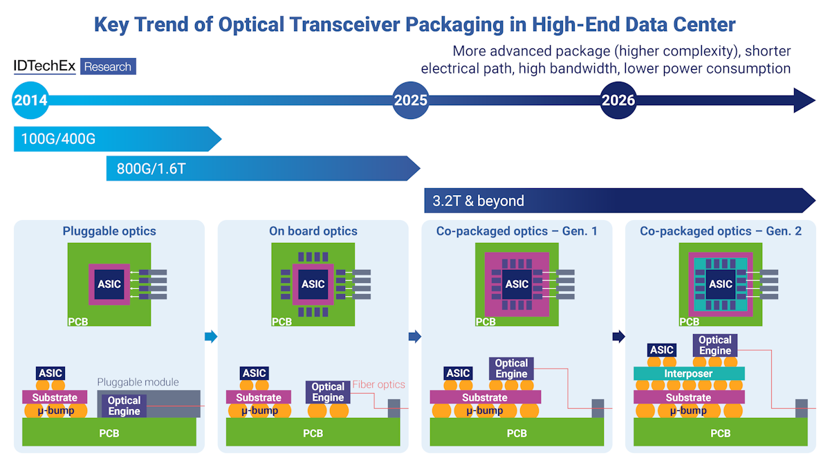
ハイエンドデータセンターにおける光トランシーバの主要トレンド。出典:IDTechEx IDTechEx
Co-Packaged Optics (CPO)における先進半導体パッケージング技術の重要性
データセンターにおけるCPOの統合は、I/O帯域幅の向上とエネルギー消費の削減を目指している。フォトニック集積回路(PIC)を電子集積回路(EIC)やスイッチICと組み合わせる方法は、パッケージング寄生素子と同様に、面およびエッジ帯域幅密度に大きな影響を与える可能性がある。これらの要因は、トランシーバーのI/O帯域幅とエネルギー効率に直接影響するため、不適切な統合はシリコンフォトニクスの利点を否定することになる。
CPOの場合、フォトニックコンポーネントとエレクトロニクスコンポーネントの統合は様々な方法で実現でき、それぞれに独自の利点と課題があります。最も先進的でまだ研究開発段階にあるのは、3Dモノリシック集積で、既存の電子プロセスノード内にフォトニックコンポーネントを最小限の変更で組み込み、アクティブフォトニクスと駆動エレクトロニクスを同じダイ内に同居させる。これにより寄生が減少し、インターフェースパッドやバンプが不要になるためパッケージングが簡素化される。しかし、モノリシック集積は一般的に古いCMOSノードを使用するため、フォトニクス性能は最適とは言えず、エネルギー消費も高くなります。このような制約はあるものの、インピーダンスの不整合は最小限に抑えられ、パッケージングも簡素化されます。
逆に、2D集積では、PICとEICをPCB上に並べて配置し、ワイヤーボンドやフリップチップで接続します。この方法は簡単でコスト効率も良いが、寄生インダクタンスが大きく、シングルエッジ接続のため集積I/Oが制限される。2D集積はパッケージングが容易である一方、ワイヤーボンドに依存するためトランシーバーの帯域幅が制限され、エネルギー消費量が増加するため、高性能アプリケーションでは効率が悪くなります。
3Dハイブリッド集積は、TSV(Through-Si-Via)、高密度ファンアウト、Cu-Cuハイブリッド・ボンディング、アクティブ・フォトニック・インターポーザーなど、さまざまな先進半導体パッケージング技術によってEICをPICの上に配置することで、寄生を大幅に低減し、より高度なソリューションを提供します。3次元集積における先進的な半導体パッケージング技術の使用は、高密度ピッチ機能を可能にし、性能を向上させる。しかし、EICから発生する熱がPICに影響を及ぼす可能性があるため、高度な熱管理ソリューションが必要となる。このような熱的課題にもかかわらず、3Dハイブリッド集積はパッケージング寄生を最小化するため、より高い性能を達成します。
2.5D集積は妥協の産物であり、EICとPICの両方をTSVによるパッシブ・インターポーザー上にフリップチップ化します。このアプローチは、3D 統合と同様に管理可能な寄生素子と高密度ピッチ機能を維持しますが、インターポーザーのトレースが必要になるため複雑さが増します。2.5D集積は、性能、コスト、製造ターンアラウンドのバランスが取れていますが、3Dハイブリッド集積よりも寄生が高くなります。
まとめると、各集積法は性能、複雑さ、コストのトレードオフを提示し、特定のアプリケーションの要件と制約に基づいた選択を導きます。
コ・パッケージド・オプティクス(CPO)市場の動向
IDTechExによると、CPO(Co-Packaged Optics)市場は2035年までに12億ドルを超え、2025年から2035年までのCAGRは28.9%と堅調に成長すると予測されている。CPOネットワークスイッチは、各スイッチが最大16個のCPO PICsを内蔵する可能性があることから、売上高を独占すると見られている。AIシステム用光インタコネクトは、市場の約20%を占めると見られており、各AIアクセラレータは、通常1個の光インタコネクトPICを利用して、先端コンピューティングアプリケーションにおける高速データ処理と通信の需要増に対応している。
.png)
2025年対2035年のCPO市場成長率。出典:IDTechEx IDTechEx
IDTechExの最新レポート「CPO(Co-Packaged Optics)2025-2035年」: 技術、市場、予測」では、コパッケージドオプティクス技術の最新の進歩を幅広く調査している。このレポートでは、主要な技術革新とパッケージング動向を深く掘り下げ、バリューチェーン全体を包括的に分析している。業界主要企業の活動を徹底的に評価し、詳細な市場予測を行い、CPOの採用が将来のデータセンターアーキテクチャの景観をどのように再構築するかを予測している。
本レポートの中心は、先端半導体パッケージがコ・パッケージド・オプティクス技術の礎石であるという認識である。IDTechExは、様々な半導体パッケージング技術がCPOの領域で果たす可能性のある役割を理解することに重点を置いている。
本レポートの主な内容は以下の通りである:
本レポートは、CPO(Co-Packaged Optics)の包括的な分析を提供し、様々な重要な側面を網羅している:
本レポートは、広範な調査と業界専門家へのインタビューに基づいており、データセンターとAI技術の未来を前進させるCo-Packaged Opticsの役割を戦略的に理解することに関心のあるすべての人に貴重な洞察を提供します。
目次 1. エグゼクティブ・サマリー 1.1. 最新の高性能AIデータセンターとはどのようなものか? 1.2. スイッチ最新のデータセンターにおける主要コンポーネント 1.3. スイッチIC帯域幅の進歩とCPO(Co-Packaged Optics)技術の必要性 1.4. データセンター・アーキテクチャにおける主要課題の概要 1.5. ハイエンドデータセンターにおける光トランシーバの主要動向 1.6. プラグケーブルと比較した場合の CPO の設計判断 1.7. 光エンジン(OE)とは 1.8. 異種集積とCPO(Co-Packaged Optics) 1.9. 半導体パッケージにおける相互接続技術の概要 1.10. 主なCPOアプリケーション:ネットワークスイッチとコンピューティング光I/O 1.11. 高度な相互接続技術による EIC/PIC 統合 1.12. 2D から 3D への EIC/PIC 統合オプション 1.13. EIC/PICの各種パッケージング技術のベンチマーク表 1.14. 3D光学エンジンとICのパッケージ例 1.15. CPO+XPU/スイッチASICの3種類のパッケージ構造 1.16. 3.光インターネットワーキング・フォーラム(OIF)が定義した2 Tb/s CPOモジュール - 1 1.17. NvidiaのSoC、HBM、EIC、PICのコ・パッケージ基板上への3D集積(TSVインターポーザ) 1.18. 異なるレーザー集積技術のベンチマーク 1.19. CPO技術の課題と将来性 1.20. CPOデモ製品のベンチマーク 1.21. IDTechExが予測する将来のAIアーキテクチャ 1.22. AIインターコネクト用光I/O CPO予測(出荷台数) 1.23. AIインターコネクト用光I/O CPO予測(売上高/市場規模) 1.24. AIアクセラレータ用CPOネットワークスイッチ(L2スイッチ)の予測(出荷台数) 1.25. AIアクセラレータ向けCPOネットワークスイッチ(L2スイッチ)の予測(市場規模・売上高) 1.26. CPO市場全体 1.27. EIC/PIC集積技術別のCPO総出荷台数(百万台) 1.28. AIアクセラレータ用ネットワークスイッチ(L2スイッチ)のシステムインテグレーション パッケージング技術別出荷台数予測 1.29. 光I/Oのシステムインテグレーション パッケージング技術別予測(出荷個数) 2. 将来のAIシステムの課題とソリューション 2.1. はじめに 2.1.1. LLMの台頭と課題 2.1.2. 最新の高性能AIデータセンターとはどのようなものか? 2.1.3. エヌビディアの最先端AIシステムに迫る 2.1.4. スイッチ最新のデータセンターにおける主要コンポーネント 2.2. ハイエンド・データセンターにおけるネットワーク・スイッチの相互接続の課題 2.2.1. ハイエンドデータセンターにおけるネットワークスイッチの相互接続技術のロードマップ 2.2.2. 高帯域幅システムにおけるセルデスのボトルネック 2.2.3. 高帯域幅システムにおけるセルデスのボトルネックに対するソリューション 2.2.4. プラガブルオプティクス - ボトルネックは何か? 2.2.5. オンボードオプティクス(OBO) 2.2.6. コ・パッケージド・オプティクス(CPO) 2.2.7. プラガブル光トランシーバー接続における伝送損失 2.2.8. プラガブル光と CPO の比較 2.2.9. プラガブルと比較した CPO の設計判断 2.2.10. スイッチ IC 帯域幅の進歩と CPO 技術の必要性 2.2.11. L2 フロントサイドネットワークアーキテクチャ図 CPO と非 CPO の比較 2.3. ハイエンドデータセンター向けコンピュートスイッチのインターコネクト(光I/O)の課題 2.3.1. AIには高性能接続が必要 2.3.2. 現在の AI システムのインターコネクトにおける銅線の数 2.3.3. AI における現在の銅線システムの限界 2.3.4. Nvidia の接続性の選択:高帯域幅システムにおける銅と光の比較 2.3.5. 高帯域幅システムにおける銅と光の比較:ベンチマーク 2.3.6. ハイエンドAIシステムにおける銅から光への相互接続 2.3.7. 現在のAIシステムアーキテクチャ 2.3.8. CuシステムによるL1バックサイド・コンピュート・アーキテクチャ 2.3.9. 光インターコネクトによるL1バックサイド・コンピュート・アーキテクチャー:Co-Packaged Optics (CPO) 2.3.10. 銅線インターコネクトを光接続に交換する機会:2.4. ハイエンドデータセンターにおける将来のAIシステム 2.4.1. 電力効率の比較:CPO対プラガブル光対銅インターコネクト 2.4.2. 60cmデータ伝送技術ベンチマークの遅延 2.4.3. IDTechExが予測する将来のAIアーキテクチャ 3. コ・パッケージド・オプティクス(CPO)入門 3.1. 本章の内容 3.2. PICの主要概念 3.2.1. フォトニック集積回路(PIC)とは? 3.2.2. PICとシリコンフォトニクスの違い 3.2.3. PICのアーキテクチャ 3.2.4. PICの利点と課題 3.3. 光エンジン(OE) 3.3.1. 光エンジンとは 3.3.2. 光エンジンの仕組み 3.3.3. 光電源 3.4. コ・パッケージド・オプティクス 3.4.1. コ・パッケージド・オプティクス(CPO)の3つの主要概念 3.4.2. CPOの主要技術構成要素 3.4.3. CPOの利点:遅延 3.4.4. CPO の利点:消費電力 3.4.5. CPO の利点:データレート 3.4.6. CPO の価値提案の概要 3.4.7. CPOにおける今後の課題 4. Co-Packaged Optics (CPO)のパッケージング 4.1. はじめに 4.1.1. 光トランシーバにパッケージされる主要コンポーネント 4.1.2. 異種集積とコ・パッケージド・フォトニクス 4.1.3. ネットワークスイッチ用CPO - パッケージングコンセプト 4.1.4. 例:1.6Tbps ネットワークスイッチ用CPO 4.1.5. XPU 用光 I/O としての CPO - パッケージングコンセプト 4.1.6. XPU用光I/OとしてのCPO-パッケージングコンセプト(続く) 4.1.7. 例コンピュートシリコン用 CPO 統合 4.1.8. CPO パッケージング技術の概要 4.2. 2.5Dおよび3D先端半導体パッケージング技術の概要と開発ロードマップ 4.2.1. 半導体パッケージングの進化ロードマップ 4.2.2. 半導体パッケージング - 技術の概要 4.2.3. 先端半導体パッケージング性能の主要指標 4.2.4. 半導体パッケージにおける相互接続技術の概要 4.2.5. 2.5D パッケージング構造の概要 4.2.6. 相互接続技術 - インターポーザ 4.2.7. パッシブインターポーザとアクティブインターポーザ 4.2.8. インターポーザーの構造RDL & スルーSi-Via 4.2.9. 2.5D 先端半導体パッケージング技術ポートフォリオ 4.3. 2.5D Siベースパッケージング技術 4.3.1. 2.Si を配線として使用する 5D パッケージング 4.3.2. 貫通電極(TSV)-現在と将来 4.3.3. 2.5次元Siベースパッケージングの開発動向 4.3.4. Si インターポーザーと Si ブリッジのベンチマーク 4.4. 2.5D 有機ベースパッケージング技術 4.4.1. 2.5D パッケージング - 高密度ファンアウト(FO)パッケージング 4.4.2. 再配線層(RDL) 4.4.3. 電子相互接続:SiO2 vs 有機誘電体 4.4.4. 2種類のファンアウト:パネルレベル 4.4.5. 2種類のファンアウト:ウェハーレベル 4.4.6. ウェーハレベルのファンアウト vs パネルレベルのファンアウト :違い 4.4.7. ファンアウトパッケージングの主要トレンド 4.4.8. 今後のファンアウトプロセスにおける課題 4.5. 2.5Dガラスベースのパッケージング技術 4.5.1. 半導体パッケージにおけるガラスの役割 4.5.2. 先端半導体パッケージのインターポーザーとしてのガラスコア 4.5.3. ガラスによるSiインターポーザーの限界の克服 4.5.4. ガラスと成形コンパウンドの比較 4.5.5. ガラスコア(インターポーザー)パッケージ - プロセスフロー 4.5.6. ガラスパッケージの課題 4.6. 3D 先端半導体パッケージング技術 4.6.1. バンプ技術の進化 4.6.2. 微細化バンプの課題 4.6.3. 先端半導体パッケージ用μバンプ 4.6.4. バンプレス Cu-Cu ハイブリッドボンディング 4.6.5. Cu-Cuハイブリッド接合の3つの方法:ベンチマーク 4.6.6. Cu-Cu ハイブリッドボンディング製造プロセスの課題 4.7. CPO パッケージング:EICとPICの統合 4.7.1. EIC/PIC集積-従来型配線技術による 4.7.2. 新しい配線技術によるEIC/PIC集積 4.7.3. 2Dから3DへのEIC/PIC集積オプション 4.7.4. EIC/PICの各種パッケージング技術のベンチマーク表 4.7.5. EIC/PICの2D集積の長所と短所 4.7.6. EIC/PICの2.5D統合の長所と短所 4.7.7. EIC/PICの3Dハイブリッド統合の長所と短所 4.7.8. EIC/PICの3Dモノリシック集積の長所と短所 4.8. EIC/PIC集積のためのTSV 4.8.1. CPOにおけるEIC/PIC統合用TSV 4.8.2. PIC と EIC の統合に TSV を使用する理由 4.8.3. シスコの光エンジンパッケージングアーキテクチャ 4.8.4. シスコ:EIC/PIC 統合用 2.5D チップオンチップ(CoC)パッケージングアーキテクチャ 4.8.5. シスコPIC/EIC 統合用 3D TSV 4.8.6. CPO における主な TSV 製造ステップと課題 - 1 4.8.7. CPOにおける主なTSV製造ステップと課題 - 2 4.8.8. シリコンフォトニクスのパッケージングオプション-TSVを使うか使わないか? 4.8.9. EIC/PIC集積用2.5D Siインターポーザーの長所と短所 4.9. EIC/PIC集積のためのファンアウト 4.9.1. ASEが提案するCPOパッケージ用ファンアウト・ソリューション 4.9.2. ASEのFOPOP-プロセス 4.9.3. CPO用FOPOPとWBパッケージの詳細分析 4.9.4. シリコンフォトニクス用光パッケージングプロセスの考察 - ASE 4.9.5. CPOにおけるPIC/EIC集積のためのSPILのFOEB(Fan-Out Embedded Bridge)構造 4.9.6. FOEB構造にPICとEICを集積するプロセスフロー 4.9.7. OEパッケージングにおけるプロセスの課題 4.9.8. ロックレー・フォトニクスはCPOパッケージング構造向けにFOWLPを提案している 4.9.9. Rockley PhotonicsのFOWLP CPOパッケージングプロセスフロー-1 4.9.10. ロックレーフォトニクスのFOWLP CPOパッケージングプロセスフロー - 2 4.9.11. EIC/PIC統合のためのファンアウト使用の課題 4.10. ガラスベースのCPOパッケージング技術 4.10.1. コーニングのビジョン 4.10.2. ガラスベースCPO - パッケージング構造 4.10.3. ガラスベース Co-packaged optics - プロセス開発 4.10.4. コーニングの 102.4 Tb/s テストビークル 4.11. EIC/PIC 統合用ハイブリッドボンディング 4.11.1. TSMC の先端半導体パッケージング技術ポートフォリオ 4.11.2. TSMC:AI向け統合HPC技術プラットフォーム 4.11.3. TSMCの光エンジン・ロードマップ - 1 4.11.4. TSMC の光エンジン・ロードマップ - 2 4.11.5. TSMC の iOIS - 統合光インターコネクション・システム 4.11.6. EICとPICを組み合わせた3D SoIC接合 4.11.7. TSMCの3D SoIC技術 4.11.8. ボンドピッチ微細化のロードマップ 4.12. OEとASIC/XPUなどのシステム統合 4.12.1. コ・パッケージングとコ・パッケージド・オプティクス(CPO)の比較 4.12.2. CPO+XPU/スイッチASICの3種類のパッケージ構造 4.12.3. 光学エンジンと集積回路(IC)を2Dまたは2.5D構成でパッケージする例 4.12.4. 2.5D構成におけるASICとのOE統合 4.12.5. 光エンジンと集積回路(IC)を3D構成でパッケージングする例 4.12.6. 将来の3D-CPO構造 4.12.7. NvidiaのSoC、HBM、EIC、PICのコ・パッケージ基板上への3D集積(TSVインターポーザ) 4.12.8. EIC/PIC の 3D 統合に基づく 51.2 Tb/s スイッチモジュールの例 4.12.9. ガラス・インターポーザー上でのEICとPICの3次元異種集積の製造プロセス 4.12.10. ガラスインターポーザー上にEIC/PICを3次元集積したスイッチモジュールの例 4.12.11. CPO技術の課題と将来の可能性 4.13. 光アライメントとレーザー集積 4.13.1. グレーティングとエッジカプラの比較:シリコンフォトニクス用高密度光I/Oの課題 4.13.2. 光アライメントの課題と解決策 - 1 4.13.3. 光アライメントの課題と解決策 - 2 4.13.4. 光アライメントの課題と解決策 - 3 4.13.5. 二つの調心アプローチ 4.13.6. 光ファイバーパッケージの複雑さの軽減 4.13.7. オンチップ光源集積方法 4.13.8. CPO用外部レーザー(1) 4.13.9. CPO用外部レーザー(2) 4.13.10. レーザーアタッチメント技術ベンチマーク - 1 4.13.11. レーザーアタッチ技術のベンチマーク - 2 4.13.12. 異なるレーザー統合技術のベンチマーク 4.13.13. 主な技術的課題:シリコン導波路とプレーナー光ファイバーとのサイズの不一致 4.13.14. ケーススタディ:CPO 用シリコンフォトニクス内蔵インターポーザー上のポリマー導波路 4.13.15. CPO用シリコンフォトニクス内蔵インターポーザーのプロセス概要 4.13.16. ポリマー光導波路付き新光有機基板 5. 主要スイッチ企業CPO の設計とロードマップ 5.1. 3.光インターネットワーキング・フォーラム(OIF)が定義した 2 Tb/s CPO モジュール - 1 5.2. 3.光インターネットワーキング・フォーラム(OIF)が定義した 2 Tb/s CPO モジュール - 1 5.3. ベンチマークされた CPO デモンストレーション製品 5.4. Cisco Co-Packaged Optics デモ 5.5. シスコCPO 電力効率 5.6. シスコ外部レーザー(ELFPP) 5.7. ブロードコム 5.8. Broadcom スイッチと Nvidia スイッチの比較 5.9. Broadcom の CPO 開発スケジュール 5.10. ブロードコムの CPO ポートフォリオ 5.11. インテル光インターコネクト 5.12. Intel Optical Compute Interconnect (2) 5.13. エヌビディアコ・パッケージド・オプティクスの機会 5.14. エヌビディア:コ・パッケージド・オプティクスの課題と最終的な考察 5.15. ラノバスの製品と進歩 5.16. UALink 5.17. Ayer Labs TeraPHY 6. 市場予測 6.1. データセンター予測手法 6.2. 世界のデータセンター人口とAIアクセラレータユニットの予測 6.3. 世界のデータセンター人口とAIアクセラレータユニット予測データ表 6.4. AIインターコネクト用光I/O CPO予測(出荷台数) 6.5. AIインターコネクト用光I/O CPO予測(売上高/市場規模) 6.6. AIアクセラレータ用CPOネットワークスイッチ(L2スイッチ)の予測(出荷台数) 6.7. AIアクセラレータ向けCPOネットワークスイッチ(L2スイッチ)データテーブル(出荷台数) 6.8. AIアクセラレータ向けCPOネットワークスイッチ(L2スイッチ)の予測(市場規模・売上高) 6.9. CPO総市場 6.10. EIC/PIC集積技術別CPO合計(出荷台数、百万台) 6.11. AIアクセラレータ用ネットワークスイッチ(L2スイッチ)のシステムインテグレーション パッケージング技術別予測(出荷台数) 6.12. 光I/Oのシステム統合 パッケージング技術別予測 (出荷個数) 6.13. パッケージング技術別CPO出荷台数予測表 7. 企業プロファイル 7.1. ACCRETECH(研削工具) 7.2. AEPONYX 7.3. Amkor ?アドバンスト・セミコンダクター・パッケージング 7.4. ASE ?アドバンスト・セミコンダクター・パッケージング 7.5. Ayar Labs:AI アクセラレータインターコネクト 7.6. CEA-Leti (アドバンスト・セミコンダクター・パッケージング) 7.7. コヒーレントフォトニック集積回路ベースのトランシーバー 7.8. EFFECTフォトニクス 7.9. EVG(3Dハイブリッドボンディングツール) 7.10. グローバルファウンドリーズ 7.11. HDマイクロシステムズ 7.12. ヘンケル(半導体パッケージング、接着技術部門) 7.13:プログラマブルフォトニック集積回路 7.14. JCETグループ 7.15. JSR株式会社 7.16. ライトインテリジェンス 7.17. ライトマター 7.18. リオニクス 7.19. リパック 7.20. LPKF 7.21. 三井金属鉱業(アドバンスト半導体パッケージング) 7.22. ナノワイヤード 7.23. レゾナック(RDL絶縁膜) 7.24. シンティル・フォトニクス 7.25. TOK 7.26. TSMC(アドバンストセミコンダクターパッケージング) 7.27. Vitron (Through-Glass Via Manufacturing) ?LPKF商標

Summary
この調査レポートは、2025-2035年のコ・パッケージド・オプティクス(CPO)市場について詳細に調査・分析しています。
主な掲載内容(目次より抜粋)
Report Summary
The rise of Co-Packaged Optics (CPO)
Over the past decade, the capacity of data center Ethernet switches has surged from 0.64 Tbps to 25.6 Tbps, driven by the adoption of 64x 400 Gbps or 32x 800 Gbps pluggable optical transceiver modules. However, these high-speed modules, within their current form factors, pose significant challenges. Issues include the required densities of electrical and optical connectors, as well as escalating power consumption.
To achieve next-generation optical engines supporting 800 Gbps and beyond per module, the communication rate must double to at least 100 Gbps per lane. This increase introduces substantial signal integrity issues across the switch socket, motherboard, and edge connector, leading to heightened power dissipation at SerDes interfaces. In future Ethernet switching, these signal integrity problems may cause I/O power consumption to exceed that of the switch core. Additionally, the integration density of standard pluggable modules is limited by the QSFP/OSFP form factor, necessitating advanced thermal management solutions not yet widely available.
Co-Packaged Optics (CPO) presents a promising solution to these challenges. Unlike traditional pluggable models, CPO integrates optical modules directly onto the switch ASIC substrate, reducing electrical reach and effectively addressing signal integrity issues. This approach has gained traction among major data centers. However, optimizing the packaging strategy for CPO remains a topic of ongoing industry discussion and development. IDTechEx's latest report, "Co-Packaged Optics 2025-2035: Technologies, Market, and Forecasts," explores these advancements in CPO technology and packaging techniques enabling its adoption.
.png)
Key trend of optical transceiver in high-end data center. Source: IDTechEx
The importance of advanced semiconductor packaging technologies for Co-Packaged Optics (CPO)
The integration of CPO in data centers aims to boost I/O bandwidth and reduce energy consumption. The way photonic integrated circuits (PICs) are combined with electronic integrated circuits (EICs) and switch ICs can significantly influence the areal and edge bandwidth density, as well as packaging parasitics. These factors directly affect the transceiver's I/O bandwidth and energy efficiency, meaning improper integration can negate the advantages of silicon photonics.
For CPO, the integration of photonic and electronic components can be achieved through various methods, each with unique advantages and challenges. The most advanced and still in the R&D phase is the 3D monolithic integration embeds photonic components within an existing electronic process node with minimal alterations, co-locating active photonics and driving electronics within the same die. This reduces parasitics and simplifies packaging by eliminating the need for interface pads and bumps. However, monolithic integration typically uses older CMOS nodes, resulting in suboptimal photonic performance and higher energy consumption. Despite these limitations, it offers minimal impedance mismatch and simplified packaging.
Conversely, 2D integration places the PIC and EIC side by side on a PCB, connected by wire bonds or flip-chip. This method is straightforward and cost-effective, but introduces significant parasitic inductance, limiting aggregate I/O due to single-edge connections. While 2D integration is easy to package, the reliance on wirebonds constrains the transceiver bandwidth and increases energy consumption, making it less efficient for high-performance applications.
3D hybrid integration offers a more advanced solution by placing the EIC on top of the PIC, via various advanced semiconductor packaging technologies, including Through-Si-Via (TSV), high density fan-out, Cu-Cu hybrid bonding, active photonic interposer, etc, significantly reducing parasitics. The use of advanced semiconductor packaging technologies in 3D integration allows for dense pitch capabilities, enhancing performance. However, thermal dissipation remains a challenge, as the heat generated by the EIC can impact the PIC, necessitating advanced thermal management solutions. Despite these thermal challenges, 3D hybrid integration achieves higher performance due to minimized packaging parasitics.
2.5D integration serves as a compromise, with both the EIC and PIC flip-chipped onto a passive interposer with TSVs. This approach maintains manageable parasitics and dense pitch capabilities similar to 3D integration but adds complexity with the need for interposer traces. While 2.5D integration balances performance, cost, and fabrication turnaround, it incurs higher parasitics than 3D hybrid integration.
In summary, each integration method presents trade-offs between performance, complexity, and cost, guiding the choice based on specific application requirements and constraints.
Co-Packaged Optics (CPO) Market trajectory
According to IDTechEx, the Co-Packaged Optics (CPO) market is projected to exceed $1.2 billion by 2035, growing at a robust CAGR of 28.9% from 2025 to 2035. CPO network switches are expected to dominate revenue generation, driven by each switch potentially incorporating up to 16 CPO PICs. Optical interconnects for AI system will constitute approximately 20% of the market, with each AI accelerator typically utilizing one optical interconnect PIC to meet increasing demands for high-speed data processing and communication in advanced computing applications.
.png)
Total CPO market growth 2025 vs 2035. Source: IDTechEx
IDTechEx's latest report, titled "Co-Packaged Optics (CPO) 2025-2035: Technologies, Market, and Forecasts," offers an extensive exploration into the latest advancements within co-packaged optics technology. The report delves deep into key technical innovations and packaging trends, providing a comprehensive analysis of the entire value chain. It thoroughly evaluates the activities of major industry players and delivers detailed market forecasts, projecting how the adoption of CPO will reshape the landscape of future data center architecture.
Central to the report is the recognition of advanced semiconductor packaging as the cornerstone of co-packaged optics technology. IDTechEx places significant emphasis on understanding the potential roles that various semiconductor packaging technologies may play within the realm of CPO.
Key aspects of the report include:
This report provides a comprehensive analysis of Co-Packaged Optics (CPO), encompassing various critical aspects:
The report is based on extensive research and interviews with industry experts and provides valuable insights for anyone interested in gaining a strategic understanding of Co-Packaged Optics' role in advancing the future of data center and AI technology.
Table of Contents
ご注文は、お電話またはWEBから承ります。お見積もりの作成もお気軽にご相談ください。本レポートと同分野の最新刊レポート
IDTechEx社の半導体、コンピュータ、AI - Semiconductors, Computing, AI分野での最新刊レポート
本レポートと同じKEY WORD()の最新刊レポート
よくあるご質問IDTechEx社はどのような調査会社ですか?IDTechExはセンサ技術や3D印刷、電気自動車などの先端技術・材料市場を対象に広範かつ詳細な調査を行っています。データリソースはIDTechExの調査レポートおよび委託調査(個別調査)を取り扱う日... もっと見る 調査レポートの納品までの日数はどの程度ですか?在庫のあるものは速納となりますが、平均的には 3-4日と見て下さい。
注文の手続きはどのようになっていますか?1)お客様からの御問い合わせをいただきます。
お支払方法の方法はどのようになっていますか?納品と同時にデータリソース社よりお客様へ請求書(必要に応じて納品書も)を発送いたします。
データリソース社はどのような会社ですか?当社は、世界各国の主要調査会社・レポート出版社と提携し、世界各国の市場調査レポートや技術動向レポートなどを日本国内の企業・公官庁及び教育研究機関に提供しております。
|
|