世界各国のリアルタイムなデータ・インテリジェンスで皆様をお手伝い

5Gと6G向け低損失材料 2024-2034年:市場、動向、予測


Low-Loss Materials for 5G and 6G 2024-2034: Markets, Trends, Forecasts

第5世代通信技術である5Gは、映画のストリーミングをより高速にするモバイル体験以上のものである。5Gは、自動車から遠隔ロボットまで、あらゆる機器間のユニバーサルな接続を可能にする。収益性の高いビジネ... もっと見る


出版社 出版年月 電子版価格 ページ数 言語
IDTechEx
アイディーテックエックス
2024年1月24日 US$7,000
電子ファイル(1-5ユーザライセンス)
ライセンス・価格情報・注文方法はこちら
380 英語

日本語のページは自動翻訳を利用し作成しています。


サマリー

第5世代通信技術である5Gは、映画のストリーミングをより高速にするモバイル体験以上のものである。5Gは、自動車から遠隔ロボットまで、あらゆる機器間のユニバーサルな接続を可能にする。収益性の高いビジネスモデルとキラーアプリケーションが出現し始める中、5Gは急成長市場の1つであり、IDTechExは2033年には8,420億米ドルを超え、世界のGDPに年間数兆ドルの接続性向上が寄与すると予測している。
 
5Gネットワークの最も革命的な側面は、26GHzから40GHzまでの周波数を利用する高周波5G技術、すなわちミリ波5Gに依存している。このような高周波数では、多くの技術やデバイスが、大幅な伝送損失、より効率的な電力供給が必要な高い電力使用量、過剰な発熱といった課題に直面している。伝送損失は、5Gアンテナと無線周波数集積回路の両方にとって悩みの種である。低周波5G、すなわち6GHz以下の5Gでは、データ転送速度が速いため、信号損失の低減も望まれる。
 
出典:IDTechEx
 
今後のmmWave 5Gの台頭により、低損失材料は急速な成長を遂げ、ますます重要な役割を果たすことになるだろう。本レポートでは、低損失材料の状況を調査し、誘電率(Dk)、誘電正接(Df)、吸湿性、コスト、製造性という5つの重要な要素によってその性能をベンチマークしている。低損失材料は、RF部品の基板やPCBに使用されるだけでなく、先進的なパッケージにも使用されます。通信技術がmmWave 5Gに向けて高周波化するにつれて、アンテナ素子のサイズは縮小し、アレイをパッケージ自体に収めることができるようになる。この統合はまた、RF経路を短縮し、伝送損失を最小化するのに役立つ。AiPでは、基板、再配線層、電磁干渉(EMI)シールド、モールドアンダーフィル(MUF)材料などに低損失材料が必要になる。
 
出典:IDTechEx
 
本レポートでは、5Gデバイス向けに有望な低損失材料に焦点を当てている。これには以下が含まれる:
  • 低損失熱硬化性材料:熱硬化性材料は、3G/4Gネットワークデバイスの市場を支配している。しかし、DkとDfが高いため、mmWave 5Gでの使用には制限がある。これらの材料のDkとDfを低減するための主要材料サプライヤーの戦略と研究開発努力に焦点を当てる。
  • ポリテトラフルオロエチレン(PTFE):自動車用レーダーシステム、高速/高周波(HS/HF)ボード、コネクターなどの高周波用途で最も一般的な材料のひとつ。
  • 液晶ポリマー(LCP):スマートフォンのアンテナ用フレキシブル基板に採用されている。同市場は今後も成長し続け、他の用途にも拡大する。
  • 低温同時焼成セラミック(LTCC): LTCCはDfが低く、Dkの範囲が広いため、小型高周波フィルターなどLTCCベースの部品の使用が加速する。
  • その他:5Gシステムの性能を最適化するため、炭化水素、ポリ(p-フェニレンエーテル)(PPEまたはPPO)、ガラスなど、さまざまな材料が使用される。これらの代替材料は、低損失5G材料市場で大きなシェアを占めるだろう。
 
さらに、6G周波数帯が割り当てられるのは数年先だが、研究機関や材料サプライヤーはすでに、次世代の通信技術に対応するために必要な材料要件を模索している。本レポートでは、さらに低いDf/Dkを達成するためのアプローチと、再構成可能なインテリジェント表面(RIS)のような潜在的な6Gアプリケーションを探求する。
 
本レポートでは、5Gデバイスの低損失材料面積と収益に焦点を当てた10年間のきめ細かな予測を、5本以上の予測線で示している。予測は以下のように区分されている:
  • 周波数:サブ6GHz 5GおよびmmWave 5G
  • 市場用途:インフラ、スマートフォン、顧客構内機器(CPE)向け低損失材料
  • 材料タイプ:サブ6GHz 5GとmmWave 5Gの両方の低損失材料の進化を探る
 
出典:IDTechEx
 
材料トレンドに基づき、2024年から2034年までの5Gデバイス向け低損失材料の収益を予測する。総市場は2034年までに21億米ドルに達する。本レポートでは、性能、技術動向、将来性、大規模展開のボトルネックなど、さまざまな観点からさまざまな低損失材料を包括的に分析している。重要な点として、本レポートは、サプライチェーン全体のプレーヤーとのインタビューを通じて収集した一次データの偏りのない分析を提示し、5Gインフラとユーザー機器のデータの大規模なデータベースを構築しています。
 
本レポートでお答えする主な質問
  • 各5Gアプリケーションで既存企業はどの低損失材料を使用しているか?
  • 各5Gアプリケーションで台頭している低損失材料は?
  • 5Gにおける各材料タイプの利点と欠点は?
  • 5Gにおける低損失材料の主要サプライヤーは?
  • 6G向け低損失材料の現状は?
  • 2024年から2034年にかけて、5G向け低損失材料の販売面積はどの程度になるのか?
  • 低損失材料の売上は周波数別、材料タイプ別にどのように推移するか?
  • 低損失材料の成長を牽引する5Gアプリケーションは?
 
主要な側面
 
本レポートでは、5Gおよび6G市場向け低損失材料の主要材料、プレーヤー、動向に関する広範な情報と分析を提供しています。
 
低損失材料の材料動向とメーカー分析:
  • 既存および新興の低損失材料の特定
  • さまざまな用途(プリント基板、フィルター、アンテナ、パッケージングなど)で使用される材料の分析
  • さまざまな材料カテゴリーにおける商品化された低損失材料の誘電特性のベンチマーク
  • 異なる材料カテゴリーにおける重要な材料サプライヤーの特定
  • 様々なアプリケーションにおける様々な材料カテゴリーの成長促進要因と限界についての議論: 5G基地局、5Gスマートフォンアンテナ、5G CPEs
  • 5G向け新技術とその低損失材料に関する議論:アンテナ・イン・パッケージ、先端半導体パッケージング、インクベースEMIシールドなど
  • 6G向け低損失材料の現状分析
 
市場予測と分析:
  • 5G向け低損失材料の10年市場予測(周波数別、用途別、材料タイプ別に細分化
  • 3つの5Gアプリケーション向け低損失材料の10年市場予測: 5G基地局、CPE、スマートフォン
  • 3つの5Gアプリケーションの5G展開と材料動向の分析


ページTOPに戻る


目次

1. 要旨
1.1. 5G、次世代セルラー通信ネットワーク
1.2. 2種類の5G:サブ6GHzとミリ波
1.3. 要約:5G/6Gの世界的動向と新たな機会
1.4. mmWave 5Gの地域別展開に関する最新情報
1.5. mmWave 5Gの地域別展開に関する最新情報
1.6. mmWave 5Gにおける低損失材料の新たな可能性
1.7. 本レポートで取り上げた5G/6G向け低損失材料
1.8. 半導体および電子機器パッケージにおける低損失材料の応用
1.9. さまざまな用途で使用される低損失材料の進化
1.10. 5G向け有機PCB材料の進化
1.11. 市販の低損失有機ラミネートのベンチマーク@10 GHz
1.12. LTCCとガラス材料のベンチマーク
1.13. 5G PCB/コンポーネント用市販低損失材料のベンチマーキング
1.14. 5G PCB/部品向け商用低損失材料の現状と展望
1.15. 主な低損失材料サプライヤーの状況
1.16. 5Gおよび6Gコネクティビティのためのパッケージング・トレンド
1.17. 5Gおよび6Gコネクティビティのためのパッケージング・トレンド
1.18. AiP用低損失材料のベンチマーク
1.19. 概要5Gスマートフォン向け先端半導体パッケージにおける再配線層
1.20. IDTechExによる6G用低損失材料の見通し
1.21. 5G向け低損失材料の展望:面積と収益
1.22. 5G向け低損失材料の周波数別予測
1.23. 5G向け低損失材料の材料タイプ別予測:売上高と面積
1.24. マーケットディスカッション5G基地局向け低損失材料
1.25. マーケットディスカッション5G用低損失材料
1.26. マーケットディスカッション5G用低損失材料スマートフォンアンテナ
1.27. マーケットディスカッション5G用低損失材料プロバイダー
1.28. 結論
2. はじめに
2.1. 用語と定義
2.1.1. IDTechExによる "基板 "の定義
2.1.2. IDTechExによる "パッケージ "の定義
2.1.3. 略語集
2.2. 5Gの紹介
2.2.1. モバイル通信の進化
2.2.2. 5G商用/プレ商用サービス(2022年)
2.2.3. 5G、次世代セルラー通信ネットワーク
2.2.4. 5G標準化ロードマップ
2.2.5. 2種類の5G:サブ6GHzとミリ波
2.2.6. 5Gネットワーク展開戦略
2.2.7. 低中帯域の5Gは、5Gの全国カバレッジを提供する最初の選択肢となることが多い。
2.2.8. 5Gの限られたカバレッジの課題を克服するためのアプローチ
2.2.9. 周波数別5G商用/プレ商用サービス
2.2.10. 5G mmWave商用/プレ商用サービス(2022年9月)
2.2.11. モバイル・プライベート・ネットワークの状況 - 周波数別
2.2.12. mmWave 5Gの地域別展開に関する最新情報
2.2.13. mmWave 5Gの地域別展開に関する最新情報
2.2.14. 5Gの主な技術革新
2.2.15. モバイル・コンシューマー向け5G市場の概要
2.2.16. 産業向け5Gの概要
2.2.17. 5Gサプライチェーンの概要
2.2.18. 5Gユーザー機器プレーヤーの状況
2.2.19. 家庭向け5G:固定無線アクセス(FWA)
2.2.20. 5G顧客宅内装置(CPE)
2.2.21. 要約:5Gの世界的動向と新たな機会
2.3. 5G用低損失材料の紹介
2.3.1. 高周波5Gデバイスの課題、トレンド、イノベーションの概要
2.3.2. mmWave 5Gにおける低損失材料の新たな可能性
2.3.3. 半導体および電子機器パッケージにおける低損失材料の応用
2.3.4. 銅張積層板の構造
2.3.5. 低損失材料の応用5G基地局におけるビームフォーミングシステム
2.3.6. 低損失材料の応用:5GにおけるPCBプロバイダー
2.3.7. 低損失素材の用途:スマートフォン用ミリ波5Gアンテナモジュール
2.3.8. 低損失材料の用途半導体パッケージ
2.3.9. mmWave 5G向け全パッケージング材料におけるDf/Dk開発のロードマップ
3. プリント基板および部品レベルの低損失材料
3.1. はじめに
3.1.1. PCBおよび半導体パッケージ用低損失材料の概要
3.1.2. 低損失材料の選択に影響する5つの重要な指標
3.2. 低損失有機ラミネートの概要
3.2.1. 一般的なポリマーの電気特性
3.2.2. 熱可塑性プラスチックと熱硬化性プラスチックの比較
3.2.3. 熱可塑性プラスチックと熱硬化性プラスチックの比較5G用
3.2.4. 5G向け有機PCB材料の進化
3.2.5. 有機高周波積層材料の技術革新動向
3.2.6. ハイブリッドシステム:高周波回路基板のコスト削減
3.2.7. 高周波・高速銅張積層板の主要サプライヤー
3.2.8. 商業化された低損失有機ラミネートのベンチマーク
3.2.9. 市販の低損失有機ラミネートのベンチマーク@10 GHz
3.2.10. その他の低損失ラミネートの例
3.3. 低損失熱硬化性樹脂
3.3.1. 低誘電損失を達成するための戦略とトレードオフ
3.3.2. 誘電損失に影響を与える要因:分極率とモル体積
3.3.3. 誘電損失に影響する因子:硬化温度
3.3.4. DkとDfを低減する戦略:極性の低い官能基または原子結合
3.3.5. DkとDfを低減する戦略:添加物
3.3.6. Dk.低減戦略かさばる構造物
3.3.7. Dk.低減戦略多孔質構造
3.3.8. Dfを減らす戦略:剛性構造
3.3.9. 変性熱硬化性樹脂のDkの限界は?
3.3.10. Dkと基板選択がPCBフィーチャーサイズに及ぼす影響
3.3.11. 高周波用途におけるPCB基板の薄型化への挑戦
3.3.12. 低損失の熱硬化性樹脂サプライヤー味の素グループ:味の素ビルドアップフィルム(ABF)
3.3.13. 低損失の熱硬化性サプライヤー:太陽インキのエポキシ系ビルドアップ材
3.3.14. 低損失の熱硬化性サプライヤー:太陽インキのエポキシ系ビルドアップ材
3.3.15. 低損失の熱硬化性樹脂サプライヤーデュポンのパイララックス積層板
3.3.16. 低損失の熱硬化性樹脂サプライヤーレアードのエコストック
3.3.17. 低損失の熱硬化性樹脂サプライヤーパナソニックのR5410
3.3.18. 低損失の熱硬化性樹脂サプライヤーJSR社の芳香族ポリエーテル(HCポリマー)
3.3.19. 低損失の熱硬化性樹脂サプライヤー昭和電工の多環式サーモセット
3.3.20. 低損失熱硬化性ラミネートのサプライヤー:三菱ガス化学のBTラミネート
3.3.21. 低損失熱硬化性ラミネートのサプライヤー:イソラ
3.3.22. 低損失熱硬化性ラミネートのサプライヤー:イソラ
3.4. 低損失熱可塑性プラスチック液晶ポリマー
3.4.1. 液晶ポリマー(LCP)
3.4.2. LCPの分類
3.4.3. スマートフォンとFPCBにおけるLCPアンテナ
3.4.4. 液晶ポリマーのサプライチェーン
3.4.5. 液晶ポリマーのサプライチェーンプリント基板用企業一覧
3.4.6. LCPの種類と主要サプライヤー
3.4.7. フレキシブルプリント回路基板のPI代替としてのLCP
3.4.8. LCP対PI:DkとDf
3.4.9. LCP対PI:水分
3.4.10. LCP対PI:柔軟性
3.4.11. LCPとMPIの比較:コスト
3.4.12. LCPとMPIの比較:FCCL信号損失
3.4.13. 市販のLCPおよびLCP-FCCL製品
3.4.14. 次世代素材スマートフォンアンテナ
3.4.15. Evolution ofスマートフォンアンテナ from2G to mmWave 5G
3.4.16. LCP製品サプライヤー村田製作所のスマートフォン向けMetroCircアンテナ
3.4.17. LCP製品サプライヤーキャリア・テクノロジー
3.4.18. LCP製品サプライヤーアバリー/ZDT
3.4.19. LCP製品のサプライヤーKGK(協同技研化学)
3.4.20. LCP製品サプライヤー:ミリ波5Gアプリケーション向けSYTECH'LCP-FCCL
3.4.21. LCP製品サプライヤー: iQLP
3.4.22. LCP製品のサプライヤーIQLPとデュポンLCP-PCB
3.5. 熱可塑性ポリマーPTFE
3.5.1. フッ素樹脂とPTFEの紹介
3.5.2. Key properties of PTFE to consider5G用 applications
3.5.3. PTFE積層板の誘電特性に及ぼす結晶化度の影響
3.5.4. 5GにおけるPTFEの主な用途
3.5.5. PTFEを基板に用いたハイブリッドカプラー
3.5.6. セラミック充填PTFEラミネートとガラス充填PTFEラミネートの比較
3.5.7. 高周波5GにPTFEベースの積層板を使用することの懸念
3.5.8. PTFEラミネートのサプライヤーロジャース' アドバンスト・コネクティビティ・ソリューションズ
3.5.9. PTFEラミネートのサプライヤー:セラミック充填PTFEラミネート
3.5.10. PTFEラミネートのサプライヤータコニック
3.5.11. PTFEラミネートのサプライヤーSYTECH
3.6. 低損失素材の持続可能性:PTFE
3.6.1. はじめにPFASへ
3.6.2. PFASの懸念
3.6.3. PFASの規制見通し:EU
3.6.4. PFASの規制見通し:アメリカ
3.6.5. PFAS物質による環境破壊に関するオランダ裁判所の判決
3.6.6. 低損失材料に関連するPFAS規制
3.7. その他の有機材料
3.7.1. ポリ(p-フェニレンオキシド)(PPO):サビック
3.7.2. ポリパラフェニレンエーテル(PPE):パナソニックのメグトロン
3.7.3. 変性ポリパラフェニレンエーテル(mPPE):旭化成のザイロン
3.7.4. ポリフェニレンサルファイド(PPS):ソルベイの基地局アンテナ用素材
3.7.5. ポリフェニレンサルファイド(PPS):東レの透明耐熱フィルム
3.7.6. ポリブチレンテレフタレート(PBT):東レ
3.7.7. 炭化水素系ラミネート
3.7.8. アンテナ基板としてのポリマーエアロゲル
3.7.9. エアロゲルのサプライヤーブルーシフト社のポリイミド・エアロゲル・ラミネート用AeroZero
3.7.10. 木材由来セルロースナノフィブリル
3.7.11. ポリカーボネート(PC):コベストロの射出成形エンクロージャおよびカバー用素材
3.8. 無機材料
3.9. セラミックス/低温同時焼成セラミックス(LTCC)
3.9.1. セラミック/LTCCの5G応用分野
3.9.2. はじめにセラミック材料へ
3.9.3. HTCCからLTCCへの進化
3.9.4. LTCC材料のベンチマーク
3.9.5. 誘電率:異なる無機基板(LTCC、ガラス)に対する安定性と周波数
3.9.6. HTCCおよびLTCCアルミナの誘電パラメーターの温度安定性
3.9.7. LTCCのサプライヤーフェロ
3.9.8. LTCCのサプライヤーデュポン
3.9.9. LTCCおよびHTCCベースの基板
3.9.10. HTCCメタルセラミックパッケージ
3.9.11. RFトランジション用LTCC基板
3.9.12. 多層LTCCパッケージの製造上の課題
3.9.13. LTCCサプライヤー京セラのLTCCパッケージ
3.9.14. LTCCサプライヤー京セラのLTCCパッケージ
3.9.15. LTCCサプライヤー京セラのLTCC応用製品と開発プロジェクト
3.9.16. SAW/BAWを超えるフィルター技術の必要性
3.9.17. mmWave 5Gに対応するフィルター技術
3.9.18. mmWave 5Gアプリケーションのための選択されたフィルター技術のベンチマーク
3.9.19. 伝送線路フィルター用材料
3.9.20. 将来のRFフィルター基板におけるLTCCとガラスの役割
3.9.21. LTCCサプライヤー日本ガイシの多層LTCCフィルター
3.9.22. LTCCサプライヤー多層LTCCフィルター
3.9.23. LTCCサプライヤーサンウェイ・コミュニケーションのミリ波5G電話用フェーズドアレイアンテナ
3.9.24. LTCCサプライヤー:テクダイヤの薄膜コンデンサとセラミックコンデンサ
3.10. ガラス
3.10.1. ガラス基板
3.10.2. Benchmark of various glass基板s
3.10.3. ガラスサプライヤーJSKの低伝送損失積層板HF-F
3.10.4. ガラスサプライヤーショットのFLEXINITYコネクト
3.10.5. ガラスサプライヤーAGC/ALCANシステムの窓用透明アンテナ
3.10.6. ガラスフィルターとして基板
3.10.7. ガラス integrated passive devices (IPD) filter5G用 by Advanced Semiconductor Engineering
3.10.8. PCBおよびRF部品用低損失材料の概要
3.10.9. 5G PCB/コンポーネント用市販低損失材料のベンチマーキング
3.10.10. 5G PCB/部品向け商用低損失材料の現状と展望
3.10.11. 低損失材料の特性概要
3.10.12. Options for mmWave filter基板s
4. パッケージレベルの低損失材料
4.1. 電子・半導体パッケージの概要
4.1.1. 一般的な電子パッケージの概要
4.1.2. 先端半導体パッケージの概要
4.1.3. From1D to3D semiconductor packaging
4.1.4. 半導体パッケージング技術の概要
4.1.5. 5Gおよび6Gコネクティビティのためのパッケージング・トレンド
4.2. システム・イン・パッケージ(SiP)
4.2.1. 異種統合ソリューション
4.2.2. システム・オン・チップ(SOC)の概要
4.2.3. マルチチップモジュール(MCM)の概要
4.2.4. システム・イン・パッケージ(SiP)
4.2.5. 分析システム・イン・パッケージ(SiP)
4.2.6. エレクトロニクスにおけるSiP含有量の増加傾向
4.3. AiP(アンテナ・イン・パッケージ)に向けて
4.3.1. 高周波集積とパッケージングのトレンド
4.3.2. Qualcomm: Antenna in package design (antenna on a基板 with flip chipped ICs)
4.3.3. クアルコムmmWave AiPの進化
4.3.4. 高周波集積とパッケージング:要件と課題
4.3.5. ミリ波アンテナ統合のための3つの方法
4.3.6. アンテナ実装技術のベンチマーク
4.3.7. AiPの開発動向
4.3.8. 2種類のAiP構造
4.3.9. 2種類のIC組み込み技術
4.3.10. 2種類のIC組み込み技術
4.3.11. IC組み込み技術の主要市場プレイヤー(技術タイプ別
4.3.12. Low loss materials: Key5G用 mmWave AiP
4.3.13. Choices of low-loss materials5G用 mmWave AiP
4.3.14. AiP用低損失材料のベンチマーク
4.3.15. Organic materials: the mainstream choice for基板s in AiP
4.3.16. LTCC AiP5G用: TDK
4.3.17. ガラス基板 AiP5G用: Georgia Tech
4.3.18. AiPの概要5G用
4.4. エポキシ樹脂モールドコンパウンド(EMC)とモールドアンダーフィル(MUF)
4.4.1. EMCとMUFとは?
4.4.2. エポキシモールディングコンパウンド(EMC)
4.4.3. EMC材料の主要パラメータ
4.4.4. 5Gアプリケーションで使用されるEMCにおける誘電率の重要性
4.4.5. 低誘電率EMC製品の実験と市販
4.4.6. エポキシ樹脂さまざまな樹脂と硬化剤システムのパラメータ
4.4.7. EMC用フィラー
4.4.8. 反り管理のためのEMC
4.4.9. EMC材料のサプライチェーン
4.4.10. EMC innovation trends5G用 applications
4.4.11. FO-WLP用高反り制御EMC
4.4.12. 反りとダイシフトに対する可能な解決策
4.4.13. EMCサプライヤー住友ベークライト
4.4.14. EMCサプライヤー住友ベークライト
4.4.15. EMCサプライヤー京セラの半導体用EMC
4.4.16. EMCサプライヤーサムスンSDI
4.4.17. EMCサプライヤー昭和電工
4.4.18. EMCサプライヤー昭和電工硫黄フリーEMC
4.4.19. EMCサプライヤーKCC株式会社
4.4.20. モールドアンダーフィル(MUF)
4.4.21. フリップクリップ成形技術に不可欠なMUF
4.4.22. 圧縮成形用液体成形コンパウンド(LMC)
4.5. インクベースのEMIシールド
4.5.1. 電磁干渉(EMI)シールドとは?
4.5.2. パッケージ・シールドにはコンパートメント・シールドとコンフォーマル・シールドがある
4.5.3. EMIシールドにはどのような素材が使われていますか?
4.5.4. 半導体パッケージ設計変更の影響
4.5.5. EMIシールド導入の主な傾向
4.5.6. スパッタリングと溶射の比較
4.5.7. 競合する印刷方法のプロセスフロー
4.5.8. サプライヤーの詳細は、スパッタリングが支配的なアプローチであることを確認している。
4.5.9. コンフォーマル・パッケージ・レベル・シールドのバリュー・チェーン
4.5.10. パッケージレベルのEMIシールド用スパッタリング
4.5.11. 結論:パッケージレベルのEMIシールドのためのスプレー/印刷
4.5.12. パッケージレベルのEMIシールドのためのその他の成膜方法
4.5.13. パッケージ・レベル・シールドの初期の商用例
4.5.14. コンパートメント化を伴うコンフォーマルパッケージレベルのEMIシールド
4.5.15. Smartphone deployment example: Conformal shielding in Apple iPhone12
4.5.16. インクベースのコンフォーマルEMIシールドを狙うサプライヤー
4.5.17. インクベースのEMIシールドサプライヤーヘンケル
4.5.18. インクベースのEMIシールドサプライヤーデュクサン
4.5.19. インクベースのEMIシールドサプライヤーニュートリアム
4.5.20. インクベースのEMIシールドサプライヤークラリアント
4.5.21. インクベースのEMIシールドサプライヤー藤倉化成
4.5.22. コンフォーマルEMIシールドに使用されるスプレーマシン
4.5.23. 粒子径と形態がEMIシールドに影響する
4.5.24. パーティクルフリーインクによるEMIシールド
4.5.25. Heraeus'インクジェット印刷による粒子フリーAgインク
4.5.26. EMIシールドの主要トレンド:複雑なパッケージのコンパートメント化
4.5.27. 低周波における磁気シールドの課題(I)
4.5.28. 低周波における磁気シールドの課題(II)
5. ウェーハレベルの低損失材料
5.1. 再分配層(RDL)
5.2. 再分配層(RDL)対シリコン
5.3. 異なるパッケージング技術における低損失RDL材料の重要性
5.4. mmWave用低損失RDL材料:TSMCのInFO AiP
5.5. RDL用高分子誘電体材料
5.6. Key parameters for organic RDL materials for next generation 2.5D fan-out packaging
5.7. RDL用有機誘電体のベンチマーク
5.8. RDL-誘電体サプライヤー東レのポリイミド材料
5.9. RDL-誘電体サプライヤーデュポンのアリールアルキルポリマー
5.10. RDL-誘電体サプライヤーデュポンのインタービア
5.11. RDL-誘電体サプライヤーHDマイクロシステムズ
5.12. RDL-誘電体サプライヤー:太陽インキのエポキシ系高密度RDL
5.13. RDL-誘電体サプライヤー味の素のナノフィラーABF
5.14. RDL-誘電体サプライヤー:昭和電工
5.15. Market for low-loss RDLs - Advanced semiconductor packages5G用スマートフォン
5.16. 概要5Gスマートフォン向け先端半導体パッケージにおける再配線層
6. 6G用低損失素材
6.1. 概要
6.1.1. モバイル通信の進化
6.1.2. 5G/6Gの開発と標準化ロードマップ
6.1.3. 6Gに関するIDTechExの見通し
6.1.4. 6G スペクトラム - どの帯域を考慮するか?
6.1.5. Spectrum outlook from2G to 6G
6.1.6. 概要潜在的な6Gサービスの
6.1.7. 6G - 主要アプリケーションの概要
6.1.8. 概要 of land-mobile service applications in the frequency range275-450 GHz
6.1.9. 要約:6Gの世界的動向と新たな機会
6.1.10. 5Gと6Gの技術革新比較
6.1.11. IDTechExによる6G用低損失材料の見通し
6.1.12. 材料カテゴリー別6G低損失材料の研究アプローチ
6.1.13. 6G用RDL材料
6.1.14. 6G用ポリイミドフィルム
6.1.15. 6G用熱可塑性プラスチック:ジョージア工科大学
6.1.16. 6G用PTFE:延世大学、GIST
6.1.17. 6G用PPS:四川大学
6.1.18. 6G用熱硬化性樹脂:ITEQコーポレーション、INAOE
6.1.19. 6G用PPE:太陽インキ、ジョージア工科大学
6.1.20. 6G用シリケート材料:オウル大学、セゲド大学
6.1.21. 6G用シリケート材料:オールボー大学、ペンシルバニア州立大学
6.1.22. 6G用シリケート材料:東京工業大学、AGC
6.1.23. ガラス6G:ジョージア工科大学
6.1.24. ガラス6G用インターポーザー
6.1.25. 6G用LTCC:フラウンホーファーIKTS
6.1.26. 6G用セラミックス:概要
6.1.27. 6G用アルミナフィラー:産業技術総合研究所
6.1.28. 6G用サステイナブル素材:オウル大学
6.1.29. Metal6G用インターポーザー: Cubic-Nuvotronics
6.1.30. 6G用低損失材料開発のロードマップ
6.1.31. 6G用低損失材料開発のロードマップ
6.1.32. 6G用低損失材料の規格
6.2. 6G用高周波メタマテリアル
6.2.1. メタマテリアルとは何か?
6.2.2. メタマテリアルの細分化
6.2.3. 6G用メタマテリアル:再構成可能なインテリジェント表面(RIS)
6.2.4. リコンフィギュラブル・インテリジェント・サーフェスの電気通信分野における主な推進要因
6.2.5. リコンフィギュラブル・インテリジェント・サーフェス(RIS)の現状
6.2.6. RISにとって重要なこと
6.2.7. RFメタマテリアルの材料選択はじめに
6.2.8. アプリケーション別動作周波数範囲
6.2.9. Comparing relevant基板 materials at low frequencies
6.2.10. Comparing relevant基板 materials at high frequencies
6.2.11. テラヘルツ近傍のアクティブRFメタマテリアルに適した材料の特定
6.2.12. PPとPTFEはPETより優れた性能を示す
6.2.13. RIS5G用/6G: Suitable RF metamaterials
6.2.14. Metamaterials in RIS5G用/6G: SWOT
7. 予測
7.1. 予測の方法と範囲
7.2. 低損失材料の予測5G用
7.2.1. 5G向け低損失材料の展望:面積と収益
7.2.2. 5G向け低損失材料の材料タイプ別予測:売上高と面積
7.2.3. 5G向け低損失材料の周波数別予測
7.2.4. マーケットディスカッション5G用低損失材料
7.3. 低損失材料の予測5G用インフラ
7.3.1. Forecast of low-loss materials5G用 base stations segmented by frequency
7.3.2. Forecast of low-loss materials5G用 base stations segmented by material
7.3.3. マーケットディスカッション5G基地局向け低損失材料
7.3.4. Forecast of low-loss materials5G用 base stations segmented by components
7.4. 低損失材料の予測5G用スマートフォン
7.4.1. Forecast of low-loss materials5G用スマートフォンアンテナ segmented by frequency
7.4.2. Forecast of low-loss materials5G用スマートフォンアンテナ segmented by material
7.4.3. マーケットディスカッション5G用低損失材料スマートフォンアンテナ
7.5. 低損失材料の予測5G用顧客構内装置(CPE)
7.5.1. Forecast of low-loss materials5G用プロバイダー segmented by frequency:面積と収益
7.5.2. Forecast of low-loss materials5G用プロバイダー segmented by material:面積と収益
7.5.3. マーケットディスカッション5G用低損失材料プロバイダー
8. 結論
8.1. 結論
9. 会社概要
10. 付録
10.1. Forecast of low-loss materials5G用 base stations segmented by materialおよびコンポーネント
10.2. Forecast for low-loss materials5G用 - Segmented by frequency and application
10.3. Forecast of low-loss materials5G用スマートフォン segmented by material
10.4. Forecast of low-loss materials5G用プロバイダー segmented by material
10.5. Forecast of low-loss materials5G用 segmented by material


ページTOPに戻る


Summary

この調査レポートでは、5Gおよび6G市場向け低損失材料の主要材料、プレーヤー、動向に関する広範な情報について詳細に調査・分析しています。
 
主な掲載内容(目次より抜粋)
  • プリント基板および部品レベルの低損失材料
  • パッケージレベルの低損失材料
  • ウェハーレベルの低損失材料
  • 6G用低損失材料
  • 予測
  • 企業プロファイル
 
Report Summary
Fifth-generation telecommunication technology, 5G, is more than a faster mobile experience to stream movies. It enables a universal connection between devices from automotive to remote robots. As profitable business models and killer applications start to emerge, 5G is one of the fastest growth markets, which IDTechEx forecasts to hit over US$842bn in 2033 and contribute trillions in annual connectivity boost to global GDP.
 
The most revolutionary aspect of the 5G network relies on high frequency 5G technologies, i.e. mmWave 5G, which utilize the spectrum from 26 GHz up to 40 GHz. At such high frequencies, many technologies and devices are facing challenges such as significant transmission loss, higher power usage needing more efficient power supply, and excess heat generation. Transmission loss is a pain point for both 5G antennas and radio frequency integrated circuits. For low frequency 5G, i.e. sub-6 GHz 5G, due to the high data transfer speed, reducing signal loss is also desirable.
 
Figure 1: Overview of challenges, trends and innovations for mmWave 5G, source: IDTechEx
 
With the future rise of mmWave 5G, low-loss materials will experience rapid growth and play an increasingly important role. In this report, we survey the landscape of the low-loss materials and benchmark their performance by five key factors, i.e. dielectric constant (Dk), dissipation factor (Df), moisture absorption, cost and manufacturability. Low-loss materials will not only be used as a substrate for RF components or for the PCB, but also within advanced packages. One strong packaging trend is antenna in package (AiP); as telecom technology goes higher in frequency towards mmWave 5G, the size of the antenna elements will shrink such that the arrays can be fitted into the package itself. This integration will also help shorten the RF paths and thus minimize the transmission losses. AiP will need low-loss materials for the substrates, redistribution layers, electromagnetic interference (EMI) shielding, mold underfill (MUF) materials, and more.
 
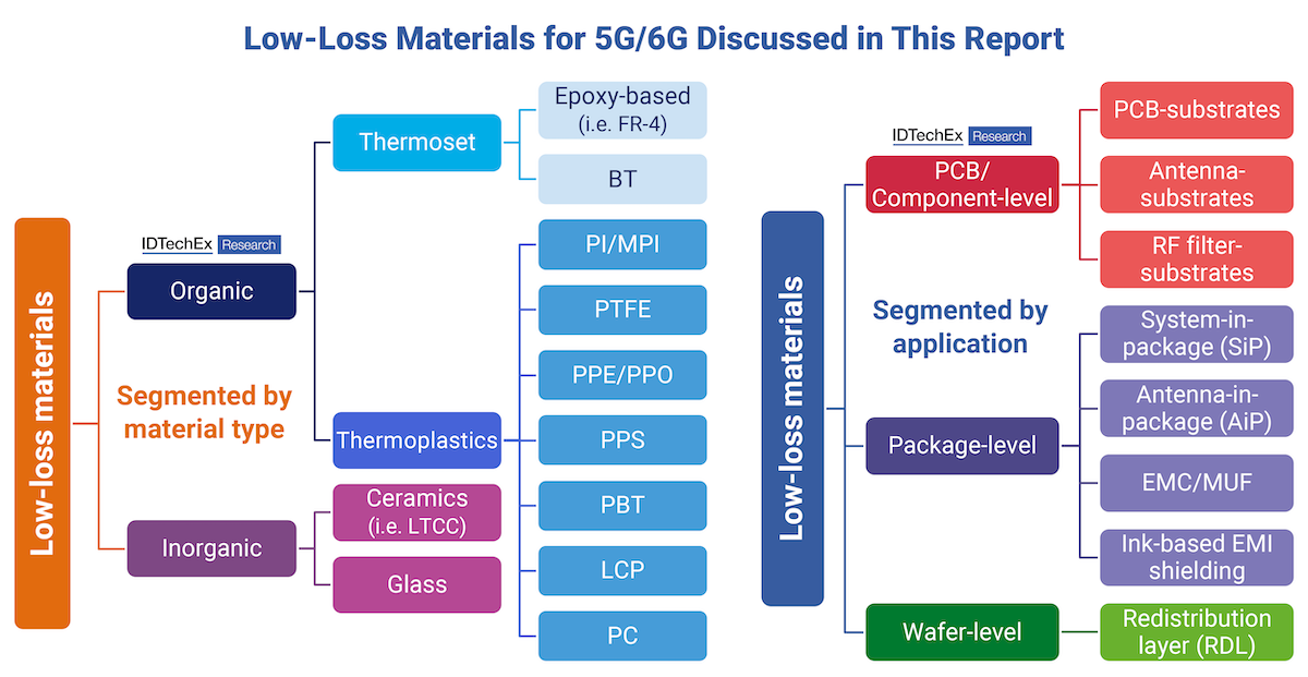
Figure 2: Scope of the low-loss materials covered in the report, source: IDTechEx
 
We highlight promising low-loss materials for 5G devices. This includes:
  • Low-loss thermoset materials: thermoset materials dominate the market for 3G/4G network devices. However, the high Dk and Df restrict their use in mmWave 5G. We focus on the strategies and R&D effort from key materials suppliers to reduce the Dk and Df for these materials
  • Polytetrafluoroethylene (PTFE): one of the most common materials for high-frequency applications such as automotive radar systems, high speed/high frequency (HS/HF) board and connectors
  • Liquid crystal polymers (LCP): it has been adapted to make flexible board for smartphone antennas. The market will continue to grow and expand into other applications
  • Low temperature co-fired ceramic (LTCC): the low Df and wide range of Dk for LTCC will accelerate the use of LTCC based components such as compact high frequency filters
  • Others: in order to optimise the performance for 5G systems, a variety of materials will be used, such as hydrocarbons, poly (p-phenylene ether) (PPE or PPO), and glass. Those alternative materials will take over a large share of the low-loss 5G materials market
 
Additionally, though the 6G spectrum is years from being allocated, research institutions and materials suppliers are already exploring the material requirements needed to meet the next generation of telecommunication technologies. This report explores the approaches to achieve even lower Df/Dk and the potential 6G applications, like reconfigurable intelligent surfaces (RIS).
 
Ten-year granular forecasts focusing on low-loss materials area and revenue for 5G devices are presented in this report, with over five forecast lines. The forecasts are segmented by:
  • Frequency: sub-6 GHz 5G and mmWave 5G
  • Market applications: low-loss materials for infrastructure, smartphone and customer premises equipment (CPE).
  • Materials type: exploring the evolution of low-loss materials for both sub-6GHz 5G and mmWave 5G
 
Figure 3: Forecast and growth rate of low-loss materials for 5G, source: IDTechEx
 
Based on materials trends, we forecast the low-loss materials revenue for 5G devices from 2024 to 2034. The total market will hit US$2.1 billion USD by 2034. The report contains a comprehensive analysis of different low-loss materials from different perspectives such as performance, technology trends, potential, and bottlenecks for large scale deployment. Importantly, the report presents an unbiased analysis of primary data gathered via our interviews with players across the supply chain, and it builds on our large database of 5G infrastructure and user equipment data.
 
Key questions answered in this report:
  • Which low-loss materials are the incumbents in each 5G application?
  • Which low-loss materials are emerging for each 5G application?
  • What are the advantages and disadvantages for each material type in 5G?
  • Who are the key suppliers for low-loss materials in 5G?
  • What is the current status of low-loss materials for 6G?
  • How much area of low-loss material for 5G will be sold between 2024 and 2034?
  • How will sales of low-loss materials evolve by frequency and material type?
  • Which 5G application will drive growth for low-loss materials?
 
Key aspects
 
This report provides extensive information and analysis on the major materials, players, and trends for low-loss materials for the 5G and 6G markets.
 
Material trends for low-loss materials and manufacturer analysis:
  • Identification of incumbent and emerging low-loss materials
  • Analysis of materials used in different applications (i.e. printed circuit boards, filters, antennas, packaging, etc.)
  • Benchmarking of dielectric properties of commercialized low-loss materials in different material categories
  • Identification of critical material suppliers for different material categories
  • Discussion of growth drivers and limitations for different material categories in different applications: 5G base stations, 5G smartphone antennas, 5G CPEs
  • Discussion of emerging technologies for 5G and their low-loss materials: antenna-in-package, advanced semiconductor packaging, ink-based EMI shielding, etc.
  • Analysis of low-loss materials for 6G and current status
 
Market Forecasts & Analysis:
  • 10-year granular market forecasts for low-loss materials for 5G, segmented by frequency, application, and material type
  • 10-year market forecasts for low-loss materials for three 5G applications: 5G base stations, CPEs, smartphones
  • Analysis of 5G deployment and material trends for three 5G applications


ページTOPに戻る


Table of Contents

1. EXECUTIVE SUMMARY
1.1. 5G, next generation cellular communications network
1.2. Two types of 5G: Sub-6 GHz and mmWave
1.3. Summary: Global trends and new opportunities in 5G/6G
1.4. Updates on mmWave 5G deployment by region
1.5. Updates on mmWave 5G deployment by region
1.6. New opportunities for low-loss materials in mmWave 5G
1.7. Low-loss materials for 5G/6G discussed in this report
1.8. Applications of low-loss materials in semiconductor and electronics packaging
1.9. Evolution of low-loss materials used in different applications
1.10. Evolution of organic PCB materials for 5G
1.11. Benchmark of commercial low-loss organic laminates @ 10 GHz
1.12. Benchmark of LTCC and glass materials
1.13. Benchmarking of commercial low-loss materials for 5G PCBs/components
1.14. Status and outlook of commercial low-loss materials for 5G PCBs/components
1.15. Key low-loss materials supplier landscape
1.16. Packaging trends for 5G and 6G connectivity
1.17. Packaging trends for 5G and 6G connectivity
1.18. Benchmark of low loss materials for AiP
1.19. Overview: Redistribution layers in advanced semiconductor packages for 5G smartphones
1.20. IDTechEx outlook of low-loss materials for 6G
1.21. Forecast of low-loss materials for 5G: Area and revenue
1.22. Forecast of low-loss materials for 5G segmented by frequency
1.23. Forecast of low-loss materials for 5G segmented by material type: Revenue and area
1.24. Market discussion: Low-loss materials for 5G base stations
1.25. Market discussion: Low-loss materials for 5G
1.26. Market discussion: Low-loss materials for 5G smartphone antennas
1.27. Market discussion: Low-loss materials for 5G CPEs
1.28. Conclusions
2. INTRODUCTION
2.1. Terms and definitions
2.1.1. IDTechEx definitions of "substrate"
2.1.2. IDTechEx definitions of "package"
2.1.3. Glossary of abbreviations
2.2. Introduction to 5G
2.2.1. Evolution of mobile communications
2.2.2. 5G commercial/pre-commercial services (2022)
2.2.3. 5G, next generation cellular communications network
2.2.4. 5G standardization roadmap
2.2.5. Two types of 5G: Sub-6 GHz and mmWave
2.2.6. 5G network deployment strategy
2.2.7. Low, mid-band 5G is often the operator's first choice to provide 5G national coverage
2.2.8. Approaches to overcome the challenges of 5G limited coverage
2.2.9. 5G Commercial/Pre-commercial Services by Frequency
2.2.10. 5G mmWave commercial/pre-commercial services (Sep. 2022)
2.2.11. Mobile private networks landscape - By frequency
2.2.12. Updates on mmWave 5G deployment by region
2.2.13. Updates on mmWave 5G deployment by region
2.2.14. The main technique innovations in 5G
2.2.15. 5G for mobile consumers market overview
2.2.16. 5G for industries overview
2.2.17. 5G supply chain overview
2.2.18. 5G user equipment player landscape
2.2.19. 5G for home: Fixed wireless access (FWA)
2.2.20. 5G Customer Premise Equipment (CPE)
2.2.21. Summary: Global trends and new opportunities in 5G
2.3. Introduction to low-loss materials for 5G
2.3.1. Overview of challenges, trends, and innovations for high frequency 5G devices
2.3.2. New opportunities for low-loss materials in mmWave 5G
2.3.3. Applications of low-loss materials in semiconductor and electronics packaging
2.3.4. Anatomy of a copper clad laminate
2.3.5. Applications of low-loss materials: Beamforming system in 5G base station
2.3.6. Applications of low-loss materials: PCBs in 5G CPEs
2.3.7. Applications for low-loss materials: mmWave 5G antenna module for smartphones
2.3.8. Applications for low-loss materials: Semiconductor packages
2.3.9. Roadmap of Df/Dk development across all packaging materials for mmWave 5G
3. LOW-LOSS MATERIALS AT THE PRINTED CIRCUIT BOARD (PCB) AND COMPONENT LEVEL
3.1. Introduction
3.1.1. Overview of low-loss materials for PCBs and semiconductor packages
3.1.2. Five important metrics impacting low-loss materials selection
3.2. Low-loss organic laminate overview
3.2.1. Electric properties of common polymers
3.2.2. Thermoplastics vs thermosets
3.2.3. Thermoplastics vs thermosets for 5G
3.2.4. Evolution of organic PCB materials for 5G
3.2.5. Innovation trends for organic high frequency laminate materials
3.2.6. Hybrid system: Cost reduction for high frequency circuit boards
3.2.7. Key suppliers for high frequency and high-speed copper clad laminate
3.2.8. Benchmark of commercialised low-loss organic laminates
3.2.9. Benchmark of commercial low-loss organic laminates @ 10 GHz
3.2.10. Other examples of low-loss laminates
3.3. Low-loss thermosets
3.3.1. Strategies to achieve lower dielectric loss and trade-offs
3.3.2. Factors affecting dielectric loss: Polarizability and molar volume
3.3.3. Factors affecting dielectric loss: curing temperature
3.3.4. Strategies to reduce Dk and Df: Low polarity functional groups or atomic bonds
3.3.5. Strategies to reduce Dk and Df: Additives
3.3.6. Strategies to reduce Dk: Bulky structures
3.3.7. Strategies to reduce Dk: Porous structures
3.3.8. Strategies to reduce Df: Rigid structures
3.3.9. Where is the limit of Dk for modified thermosets?
3.3.10. The influence of Dk and substrate choice on PCB feature size
3.3.11. The challenge of thinning the PCB-substrate for high frequency applications
3.3.12. Low-loss thermoset suppliers: Ajinomoto Group's Ajinomoto Build Up Film (ABF)
3.3.13. Low-loss thermoset suppliers: Taiyo Ink's epoxy-based build-up materials
3.3.14. Low-loss thermoset suppliers: Taiyo Ink's epoxy-based build-up materials
3.3.15. Low-loss thermoset suppliers: DuPont's Pyralux laminates
3.3.16. Low-loss thermoset suppliers: Laird's ECCOSTOCK
3.3.17. Low-loss thermoset suppliers: Panasonic's R5410
3.3.18. Low-loss thermoset suppliers: JSR Corp's aromatic polyether (HC polymer)
3.3.19. Low-loss thermoset suppliers: Showa Denko's polycyclic thermoset
3.3.20. Low-loss thermoset laminate suppliers: Mitsubishi Gas Chemical's BT laminate
3.3.21. Low-loss thermoset laminate suppliers: Isola
3.3.22. Low-loss thermoset laminate suppliers: Isola
3.4. Low-loss thermoplastics: Liquid crystal polymers
3.4.1. Liquid crystal polymers (LCP)
3.4.2. LCP classification
3.4.3. LCP antennas in smartphones and FPCBs
3.4.4. Liquid crystal polymer supply chain
3.4.5. Liquid crystal polymer supply chain for printed circuit boards: Companies
3.4.6. LCP types and key suppliers
3.4.7. LCP as an alternative to PI for flexible printed circuit boards
3.4.8. LCP vs PI: Dk and Df
3.4.9. LCP vs PI: Moisture
3.4.10. LCP vs PI: Flexibility
3.4.11. LCP vs MPI: Cost
3.4.12. LCP vs MPI: FCCL signal loss
3.4.13. Commercial LCP and LCP-FCCL products
3.4.14. Next-generation materials for smartphone antennas
3.4.15. Evolution of smartphone antennas from 2G to mmWave 5G
3.4.16. LCP product suppliers: Murata's MetroCirc antennas for smartphones
3.4.17. LCP product suppliers: Career Technology
3.4.18. LCP product suppliers: Avary/ZDT
3.4.19. LCP product suppliers: KGK (Kyodo Giken Kagaku)
3.4.20. LCP product suppliers: SYTECH's LCP-FCCL for mmWave 5G applications
3.4.21. LCP product suppliers: iQLP
3.4.22. LCP product suppliers: IQLP and DuPont's LCP-PCB
3.5. Thermoplastic polymer: PTFE
3.5.1. An introduction to fluoropolymers and PTFE
3.5.2. Key properties of PTFE to consider for 5G applications
3.5.3. Effect of crystallinity on the dielectric properties of PTFE-based laminates
3.5.4. Key applications of PTFE in 5G
3.5.5. Hybrid couplers using PTFE as a substrate
3.5.6. Ceramic-filled vs glass-filled PTFE laminates
3.5.7. Concerns of using PTFE-based laminates for high frequency 5G
3.5.8. PTFE laminate suppliers: Rogers' Advanced Connectivity Solutions
3.5.9. PTFE laminate suppliers: Rogers' ceramic-filled PTFE laminates
3.5.10. PTFE laminate suppliers: Taconic
3.5.11. PTFE laminate suppliers: SYTECH
3.6. Sustainability in low-loss materials: PTFE
3.6.1. Introduction to PFAS
3.6.2. Concerns with PFAS
3.6.3. Regulatory outlook for PFAS: EU
3.6.4. Regulatory outlook for PFAS: USA
3.6.5. Dutch court ruling on environmental damage caused by PFAS materials
3.6.6. Regulations on PFAS as relevant to low-loss materials
3.7. Other organic materials
3.7.1. Poly(p-phenylene oxide) (PPO): Sabic
3.7.2. Poly(p-phenylene ether) (PPE): Panasonic's MEGTRON
3.7.3. Modified poly(p-phenylene ether) (mPPE): Asahi Kasei's XYRON
3.7.4. Polyphenylene sulfide (PPS): Solvay's materials for base station antennas
3.7.5. Polyphenylene sulfide (PPS): Toray's transparent, heat-resistant film
3.7.6. Polybutylene terephthalate (PBT): Toray
3.7.7. Hydrocarbon-based laminates
3.7.8. Polymer aerogels as antenna substrates
3.7.9. Aerogel suppliers: Blueshift's AeroZero for polyimide aerogel laminates
3.7.10. Wood-derived cellulose nanofibril
3.7.11. Polycarbonate (PC): Covestro's materials for injection-molded enclosures and covers
3.8. Inorganic materials
3.9. Ceramics/low-temperature co-fired ceramics (LTCC)
3.9.1. 5G application areas for ceramics/LTCC
3.9.2. Introduction to ceramic materials
3.9.3. The evolution from HTCC to LTCC
3.9.4. Benchmark of LTCC materials
3.9.5. Dielectric constant: Stability vs frequency for different inorganic substrates (LTCC, glass)
3.9.6. Temperature stability of dielectric parameters of HTCC and LTCC alumina
3.9.7. LTCC suppliers: Ferro
3.9.8. LTCC suppliers: DuPont
3.9.9. LTCC and HTCC-based substrates
3.9.10. HTCC metal-ceramic packages
3.9.11. LTCC substrate for RF transitions
3.9.12. Production challenges of multilayer LTCC package
3.9.13. LTCC suppliers: Kyocera's LTCC-based packages
3.9.14. LTCC suppliers: Kyocera's LTCC-based packages
3.9.15. LTCC suppliers: Kyocera's LTCC-based products and development projects
3.9.16. Need for filter technologies beyond SAW/BAW
3.9.17. Filter technologies compatible with mmWave 5G
3.9.18. Benchmark of selected filter technologies for mmWave 5G applications
3.9.19. Materials for transmission-line filters
3.9.20. Role of LTCC and glass for future RF filter substrates
3.9.21. LTCC suppliers: NGK's multi-layer LTCC filters
3.9.22. LTCC suppliers: Minicircuits' multilayer LTCC filter
3.9.23. LTCC suppliers: Sunway communication's phased array antenna for mmWave 5G phones
3.9.24. LTCC suppliers: Tecdia's thin film and ceramic capacitors
3.10. Glass
3.10.1. Glass substrate
3.10.2. Benchmark of various glass substrates
3.10.3. Glass suppliers: JSK's HF-F for low transmission loss laminates
3.10.4. Glass suppliers: SCHOTT's FLEXINITY connect
3.10.5. Glass suppliers: AGC/ALCAN System's transparent antennas for windows
3.10.6. Glass as a filter substrate
3.10.7. Glass integrated passive devices (IPD) filter for 5G by Advanced Semiconductor Engineering
3.10.8. Summary of low-loss materials for PCBs and RF components
3.10.9. Benchmarking of commercial low-loss materials for 5G PCBs/components
3.10.10. Status and outlook of commercial low-loss materials for 5G PCBs/components
3.10.11. Property overview of low-loss materials
3.10.12. Options for mmWave filter substrates
4. LOW-LOSS MATERIALS AT THE PACKAGE-LEVEL
4.1. Overview of electronic and semiconductor packaging
4.1.1. Overview of general electronic packaging
4.1.2. Overview of advanced semiconductor packaging
4.1.3. From 1D to 3D semiconductor packaging
4.1.4. Overview of semiconductor packaging technologies
4.1.5. Packaging trends for 5G and 6G connectivity
4.2. System in package (SiP)
4.2.1. Heterogeneous integration solutions
4.2.2. Overview of System on Chip (SOC)
4.2.3. Overview of Multi-Chip Module (MCM)
4.2.4. System in Package (SiP)
4.2.5. Analysis of System in Package (SiP)
4.2.6. Trend of increasing SiP content in electronics
4.3. Towards AiP (antenna in package)
4.3.1. High frequency integration and packaging trend
4.3.2. Qualcomm: Antenna in package design (antenna on a substrate with flip chipped ICs)
4.3.3. Evolution of Qualcomm mmWave AiP
4.3.4. High frequency integration and packaging: Requirements and challenges
4.3.5. Three methods for mmWave antenna integration
4.3.6. Benchmarking of antenna packaging technologies
4.3.7. AiP development trend
4.3.8. Two types of AiP structures
4.3.9. Two types of IC-embedded technology
4.3.10. Two types of IC-embedded technology
4.3.11. Key market players for IC-embedded technology by technology type
4.3.12. Low loss materials: Key for 5G mmWave AiP
4.3.13. Choices of low-loss materials for 5G mmWave AiP
4.3.14. Benchmark of low loss materials for AiP
4.3.15. Organic materials: the mainstream choice for substrates in AiP
4.3.16. LTCC AiP for 5G: TDK
4.3.17. Glass substrate AiP for 5G: Georgia Tech
4.3.18. Summary of AiP for 5G
4.4. Epoxy molded compounds (EMC) and mold under fill (MUF)
4.4.1. What are EMC and MUFs?
4.4.2. Epoxy Molding Compound (EMC)
4.4.3. Key parameters for EMC materials
4.4.4. Importance of dielectric constant for EMC used in 5G applications
4.4.5. Experimental and commercial EMC products with low dielectric constant
4.4.6. Epoxy resin: Parameters of different resins and hardener systems
4.4.7. Fillers for EMC
4.4.8. EMC for warpage management
4.4.9. Supply chain for EMC materials
4.4.10. EMC innovation trends for 5G applications
4.4.11. High warpage control EMC for FO-WLP
4.4.12. Possible solutions for warpage and die shift
4.4.13. EMC suppliers: Sumitomo Bakelite
4.4.14. EMC suppliers: Sumitomo Bakelite
4.4.15. EMC suppliers: Kyocera's EMCs for semiconductors
4.4.16. EMC suppliers: Samsung SDI
4.4.17. EMC suppliers: Showa Denko
4.4.18. EMC suppliers: Showa Denko's sulfur-free EMC
4.4.19. EMC suppliers: KCC Corporation
4.4.20. Molded underfill (MUF)
4.4.21. MUF critical for flip clip molding technology
4.4.22. Liquid molding compound (LMC) for compression molding
4.5. Ink-based EMI shielding
4.5.1. What is electromagnetic interference (EMI) shielding?
4.5.2. Package shielding involves compartmental and conformal shielding
4.5.3. What materials are used for EMI shielding?
4.5.4. Impact of changes in semiconductor package design
4.5.5. Key trends for EMI shielding implementation
4.5.6. Comparison of sputtering and spraying
4.5.7. Process flow for competing printing methods
4.5.8. Supplier details confirm that sputtering is the dominant approach
4.5.9. Value chain for conformal package-level shielding
4.5.10. Sputtering for package-level EMI shielding
4.5.11. Conclusions: Spraying/printing for package-level EMI shielding
4.5.12. Other deposition methods for package-level EMI shielding
4.5.13. Early commercial example of package-level shielding
4.5.14. Conformal package-level EMI shielding accompanied by compartmentalization
4.5.15. Smartphone deployment example: Conformal shielding in Apple iPhone 12
4.5.16. Suppliers targeting ink-based conformal EMI shielding
4.5.17. Ink-based EMI shielding suppliers: Henkel
4.5.18. Ink-based EMI shielding suppliers: Duksan
4.5.19. Ink-based EMI shielding suppliers: Ntrium
4.5.20. Ink-based EMI shielding suppliers: Clariant
4.5.21. Ink-based EMI shielding suppliers: Fujikura Kasei
4.5.22. Spray machines used in conformal EMI shielding
4.5.23. Particle size and morphology influence EMI shielding
4.5.24. EMI shielding with particle-free inks
4.5.25. Heraeus' inkjet printed particle-free Ag inks
4.5.26. Key trend for EMI shielding: Compartmentalization of complex packages
4.5.27. The challenge of magnetic shielding at low frequencies (I)
4.5.28. The challenge of magnetic shielding at low frequencies (II)
5. LOW-LOSS MATERIALS AT THE WAFER-LEVEL
5.1. Redistribution layer (RDL)
5.2. Redistribution layer (RDL) vs silicon
5.3. Importance of low-loss RDL materials for different packaging technologies
5.4. Low-loss RDL materials for mmWave: TSMC's InFO AiP
5.5. Polymer dielectric materials for RDL
5.6. Key parameters for organic RDL materials for next generation 2.5D fan-out packaging
5.7. Benchmark of organic dielectrics for RDL
5.8. RDL-dielectric suppliers: Toray's polyimide materials
5.9. RDL-dielectric suppliers: DuPont's Arylalkyl polymers
5.10. RDL-dielectric suppliers: DuPont's InterVia
5.11. RDL-dielectric suppliers: HD Microsystems
5.12. RDL-dielectric suppliers: Taiyo Ink's epoxy-based high-density RDL
5.13. RDL-dielectric suppliers: Ajinomoto's nanofiller ABF
5.14. RDL-dielectric supplier: Showa Denko
5.15. Market for low-loss RDLs - Advanced semiconductor packages for 5G smartphones
5.16. Overview: Redistribution layers in advanced semiconductor packages for 5G smartphones
6. LOW-LOSS MATERIALS FOR 6G
6.1. Overview
6.1.1. Evolution of mobile communications
6.1.2. 5G/6G development and standardization roadmap
6.1.3. IDTechEx outlook for 6G
6.1.4. 6G spectrum - Which bands are considered?
6.1.5. Spectrum outlook from 2G to 6G
6.1.6. Overview of potential 6G services
6.1.7. 6G - An overview of key applications
6.1.8. Overview of land-mobile service applications in the frequency range 275-450 GHz
6.1.9. Summary: Global trends and new opportunities in 6G
6.1.10. Technical innovation comparison between 5G and 6G
6.1.11. IDTechEx outlook of low-loss materials for 6G
6.1.12. Research approaches for 6G low-loss materials by material category
6.1.13. RDL materials for 6G
6.1.14. Polyimide films for 6G
6.1.15. Thermoplastics for 6G: Georgia Tech
6.1.16. PTFE for 6G: Yonsei University, GIST
6.1.17. PPS for 6G: Sichuan University
6.1.18. Thermosets for 6G: ITEQ Corporation, INAOE
6.1.19. PPE for 6G: Taiyo Ink, Georgia Institute of Technology
6.1.20. Silicate materials for 6G: University of Oulu, University of Szeged
6.1.21. Silicate materials for 6G: Aalborg University, Penn State
6.1.22. Silicate materials for 6G: Tokyo Institute of Technology, AGC
6.1.23. Glass for 6G: Georgia Tech
6.1.24. Glass interposers for 6G
6.1.25. LTCC for 6G: Fraunhofer IKTS
6.1.26. Ceramics for 6G: overview
6.1.27. Alumina fillers for 6G: National Institute of Advanced Industrial Science and Technology
6.1.28. Sustainable materials for 6G: University of Oulu
6.1.29. Metal interposers for 6G: Cubic-Nuvotronics
6.1.30. Roadmap for development of low-loss materials for 6G
6.1.31. Roadmap for development of low-loss materials for 6G
6.1.32. Standards for low-loss materials for 6G
6.2. Radio-frequency metamaterials for 6G
6.2.1. What is a metamaterial?
6.2.2. Segmenting the metamaterial landscape
6.2.3. Metamaterials for 6G: Reconfigurable intelligent surfaces (RIS)
6.2.4. Key drivers for reconfigurable intelligent surfaces in telecommunications
6.2.5. The current status of reconfigurable intelligent surfaces (RIS)
6.2.6. Key takeaways for RIS
6.2.7. Materials selection for RF metamaterials: Introduction
6.2.8. Operational frequency ranges by application
6.2.9. Comparing relevant substrate materials at low frequencies
6.2.10. Comparing relevant substrate materials at high frequencies
6.2.11. Identifying suitable materials for active RF metamaterials near THz
6.2.12. PP and PTFE show better performance than PET
6.2.13. RIS for 5G/6G: Suitable RF metamaterials
6.2.14. Metamaterials in RIS for 5G/6G: SWOT
7. FORECASTS
7.1. Forecast methodology and scope
7.2. Low-loss material forecasts for 5G
7.2.1. Forecast of low-loss materials for 5G: Area and revenue
7.2.2. Forecast of low-loss materials for 5G segmented by material type: Revenue and area
7.2.3. Forecast of low-loss materials for 5G segmented by frequency
7.2.4. Market discussion: Low-loss materials for 5G
7.3. Low-loss material forecasts for 5G infrastructure
7.3.1. Forecast of low-loss materials for 5G base stations segmented by frequency
7.3.2. Forecast of low-loss materials for 5G base stations segmented by material
7.3.3. Market discussion: Low-loss materials for 5G base stations
7.3.4. Forecast of low-loss materials for 5G base stations segmented by components
7.4. Low-loss material forecasts for 5G smartphones
7.4.1. Forecast of low-loss materials for 5G smartphone antennas segmented by frequency
7.4.2. Forecast of low-loss materials for 5G smartphone antennas segmented by material
7.4.3. Market discussion: Low-loss materials for 5G smartphone antennas
7.5. Low-loss material forecasts for 5G customer premises equipment (CPEs)
7.5.1. Forecast of low-loss materials for 5G CPEs segmented by frequency: Area and revenue
7.5.2. Forecast of low-loss materials for 5G CPEs segmented by material: Area and revenue
7.5.3. Market discussion: Low-loss materials for 5G CPEs
8. CONCLUSION
8.1. Conclusions
9. COMPANY PROFILES
10. APPENDIX
10.1. Forecast of low-loss materials for 5G base stations segmented by material and component
10.2. Forecast for low-loss materials for 5G - Segmented by frequency and application
10.3. Forecast of low-loss materials for 5G smartphones segmented by material
10.4. Forecast of low-loss materials for 5G CPEs segmented by material
10.5. Forecast of low-loss materials for 5G segmented by material


ページTOPに戻る

ご注文は、お電話またはWEBから承ります。お見積もりの作成もお気軽にご相談ください。

webからのご注文・お問合せはこちらのフォームから承ります

本レポートと同分野の最新刊レポート

  • 本レポートと同分野の最新刊レポートはありません。

本レポートと同じKEY WORD(6G)の最新刊レポート

  • 本レポートと同じKEY WORDの最新刊レポートはありません。

よくあるご質問


IDTechEx社はどのような調査会社ですか?


IDTechExはセンサ技術や3D印刷、電気自動車などの先端技術・材料市場を対象に広範かつ詳細な調査を行っています。データリソースはIDTechExの調査レポートおよび委託調査(個別調査)を取り扱う日... もっと見る


調査レポートの納品までの日数はどの程度ですか?


在庫のあるものは速納となりますが、平均的には 3-4日と見て下さい。
但し、一部の調査レポートでは、発注を受けた段階で内容更新をして納品をする場合もあります。
発注をする前のお問合せをお願いします。


注文の手続きはどのようになっていますか?


1)お客様からの御問い合わせをいただきます。
2)見積書やサンプルの提示をいたします。
3)お客様指定、もしくは弊社の発注書をメール添付にて発送してください。
4)データリソース社からレポート発行元の調査会社へ納品手配します。
5) 調査会社からお客様へ納品されます。最近は、pdfにてのメール納品が大半です。


お支払方法の方法はどのようになっていますか?


納品と同時にデータリソース社よりお客様へ請求書(必要に応じて納品書も)を発送いたします。
お客様よりデータリソース社へ(通常は円払い)の御振り込みをお願いします。
請求書は、納品日の日付で発行しますので、翌月最終営業日までの当社指定口座への振込みをお願いします。振込み手数料は御社負担にてお願いします。
お客様の御支払い条件が60日以上の場合は御相談ください。
尚、初めてのお取引先や個人の場合、前払いをお願いすることもあります。ご了承のほど、お願いします。


データリソース社はどのような会社ですか?


当社は、世界各国の主要調査会社・レポート出版社と提携し、世界各国の市場調査レポートや技術動向レポートなどを日本国内の企業・公官庁及び教育研究機関に提供しております。
世界各国の「市場・技術・法規制などの」実情を調査・収集される時には、データリソース社にご相談ください。
お客様の御要望にあったデータや情報を抽出する為のレポート紹介や調査のアドバイスも致します。


詳細検索

このレポートへのお問合せ

03-3582-2531

電話お問合せもお気軽に


2024/06/28 10:26

162.07 円

173.83 円

207.48 円

ページTOPに戻る