Quantum Dot Materials and Technologies 2024-2034: Trends, Markets, Applications量子ドット材料と技術 2024-2034:トレンド、市場、アプリケーション この調査レポートでは、2024-2034年の量子ドット材料と技術について詳細に調査・分析しています。 主な掲載内容(目次より抜粋) 量子ドット材料の最適化 QD光強化ディスプ... もっと見る
※ 調査会社の事情により、予告なしに価格が変更になる場合がございます。
Summary
この調査レポートでは、2024-2034年の量子ドット材料と技術について詳細に調査・分析しています。
主な掲載内容(目次より抜粋)
Report Summary
Quantum dots (QDs) are semiconductor nanocrystals in the range of 2-10 nanometers (10-50 atoms) with size-tunable features. They exhibit quantum confinement effects due to their nanoscale dimensions, leading to remarkable optical and electrical characteristics. The quantum dot features can be adjusted by particle size, material, and compositions. QD materials such as Cd-based, In-based, PbS, perovskites, as well as emerging CuInS2, InAs, ZnTeSe QDs have varied bandgap and thus absorption and emission spectra. This fine-tune ability has resulted in quantum dots having significant application potential, notably in display, image sensor, photovoltaic, lighting and various other use cases.
Since they were first discovered in 1980, QDs have demonstrated immense potential in transforming display, image sensor, photovoltaic, lighting, and greenhouse film technologies with commercial products.
This report provides IDTechEx's technology roadmap considering how the technology mix in various applications will be transformed with time.
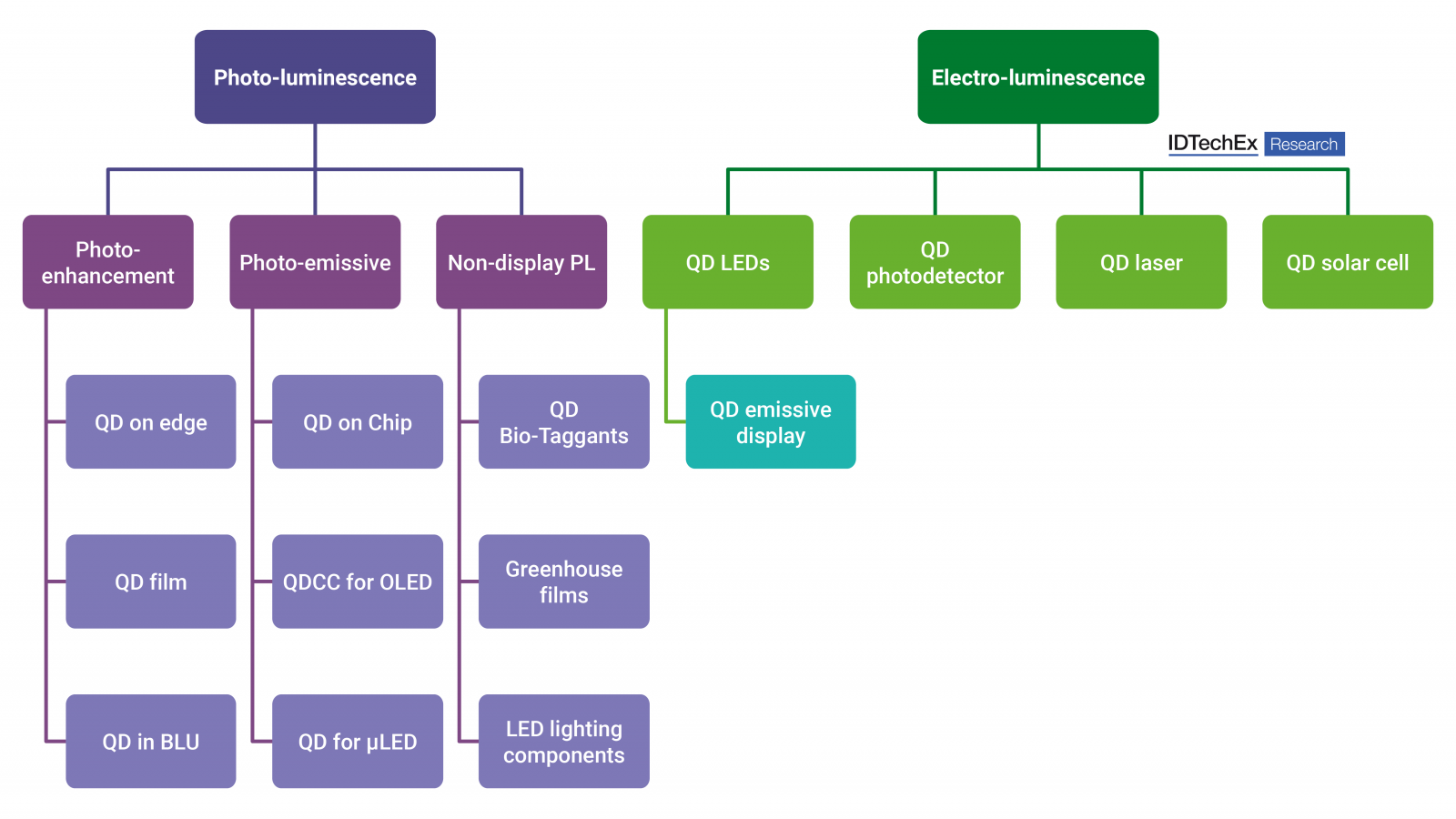
Display: Successful Application?
In display technology, QDs have found extensive use as a color-enhancing component offering a wider color gamut, higher color accuracy, and increased brightness compared to a traditional liquid crystal display (LCD). The unique photoluminescent property of emitting specific wavelengths of light upon excitation enables QDs to convert blue light from LEDs into pure red and green, thus achieving a more extensive and precise color palette.
The evolution of QD integration approaches in displays is examined in the report, highlighting the dominance of the film-type adoption over the obsolete edge optic. Nevertheless, emerging approaches such as QD color filters for OLED and micro-LED (μLED) or on-chip type are gaining momentum, facilitated by material advancements and fabrication technique improvement, which could eventually surpass the film-type. Additionally, this analysis recognizes QDs as the ultimate emissive material for displays, tracking efficiency and lifetime improvements while delving into persistent challenges regarding performance, lifetime, deposition/patterning, and device design.
.png) 
Various QD adoption in displays
Source: IDTechEx
Emerging Dominance: Quantum Dots in Image Sensors?
Lead sulfide QDs offer the advantage of tunability across an extensive spectrum of wavelengths, making them suitable for near-infrared (NIR) or short-wave infrared (SWIR) sensing applications. An intriguing possibility arises as they can be combined with a silicon Read-Out Integrated Circuit (ROIC) to form a hybrid QD-Si NIR/SWIR image sensor. This innovative integration presents a potential pathway towards achieving high-resolution small-pixel silicon-based NIR/SWIR sensors, eliminating the necessity for heterogeneous hybridization of indium gallium arsenide (InGaAs) sensors with Si ROIC. The low-cost hybrid QD-based image sensors can not only target applications traditionally realized by InGaAs SWIR image sensors, but also help to reach new applications.
With the first generation of products already on the market and giants also getting involved in this area, the promise of this technology remains strong. This report explores hybrid QD-Si image sensors that can simultaneously achieve high resolution, low pixel pitch and global shutter with potentially low-costs. Technology analysis and player introductions are provided as well.
Quantum Dots: Illuminating the Future of Lighting?
Existing commercial products are based on QDs' photoluminescent features and have demonstrated remarkable potential in lighting technologies. They can be integrated into LED lighting systems as color converters, enabling the production of tunable and high-quality white light. QD-based LEDs can achieve excellent color rendering indices (CRI) and color temperatures, making them suitable for a variety of lighting applications, including indoor and automotive lighting. Moreover, the narrow emission spectra of QDs reduce the need for complex filtering, enhancing energy efficiency and reducing light pollution.
Quantum Dots in Photovoltaics: Yes or No?
QDs can be potentially integrated into photovoltaic (PV) devices, leading to the emergence of third-generation solar cells. By engineering the bandgap of quantum dots to match specific regions of the solar spectrum, these cells can efficiently capture a broader range of light wavelengths, as well as enable multiple exciton generation (MEG) effect, allowing improved light harvesting, higher conversion efficiencies, and better performance under low-light conditions. They can also offer the potential for flexible and transparent photovoltaic applications. The report benchmarked various PV technologies, exploring commercial and technical challenges that need to be overcome.
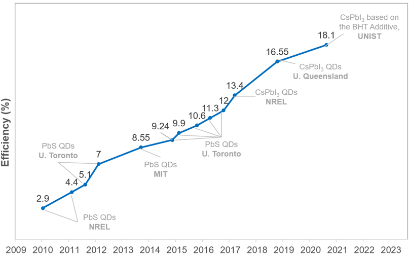
QD PV efficiency records
Data sourced from NREL Solar PV Efficiency Chart, plotted by IDTechEx
Quantum Dots: Changing and Expanding Applications?
QDs can provide added values to existing technologies in various applications from both their photoluminescent and electroluminescent features. The potential to reshuffle the supply chain for different case cases also brings up new opportunities to relevant players.
With in-depth technological research and analysis on the QD topic, the report provides data-driven evaluation, insights from our years of accumulation on QD topic research. Our roadmap comprehensively examines the integration of QDs for various applications with outlook. Challenges such as toxicity concerns, long-term stability, and large-scale manufacturing techniques and costs must be addressed. Researchers are actively exploring non-toxic and more stable materials to overcome these hurdles. Additionally, advancements in QD synthesis techniques and manufacturing processes are likely to drive down production costs and promote widespread adoption in commercial applications.
This report also provides 10-year market forecasts in area (square meter), weight (ton) and value, and at material level, for 11 application sectors including LCD TV, miniLED backlight displays, QD-OLED TVs, QD-μLED TVs, on-chip type, emissive QLED displays, photodetectors, lighting, agricultural films, research and other.
IDTechEx's forecasts draw heavily from its technology analysis which gives realistic and expert views of when and how various technologies can become commercially viable compared incumbents, as well as detailed interviews, deep market insights, and close trend tracking.
.png)
IDTechEx forecast of global QD materials market. Source: IDTechEx
IDTechEx Research has been analyzing the technologies and markets for quantum dots since 2013. Since that time, it has stayed extremely close to the latest research and market developments via its interview program and company and conference visits.
Furthermore, IDTechEx Research has engaged closely with many of its clients, helping them better understand the technology and market landscape and helping them set up their innovation and commercialization strategies.
In its analysis of quantum dots, IDTechEx Research brings its wealth of expertise in analyzing advanced electronic materials and devices. Over the past 20 years IDTechEx has closely observed the rise and/or fall, and the success and/or disappointment, of many emerging technologies.
This gives IDTechEx uniquely experienced eye when it comes to analyzing emerging electronic material technologies. This is crucial because it helps us establish a realistic market and technology roadmap that reflects the true potential of the technology based on its intrinsic characteristics and on the true level of technical and commercial challenges that it faces.
Table of Contents
株式会社 データリソース Data Resource, Inc.
電話:03-3582-2531
COPYRIGHT(C) 2011-2025 DATA RESOURCE, Inc. ALL RIGHTS RESERVED. |